Power semiconductor module

a technology of semiconductor modules and semiconductors, applied in semiconductor devices, semiconductor/solid-state device details, electrical apparatus, etc., can solve the problems of limiting the thermal or thermodynamic capability of the semiconductor, the force is not directly normal to the interface between the semiconductor and the cooled surface, and the relative large volume of the housing, so as to achieve the effect of simple production of such modules and high yield in the mounting of sub-assemblies

Active Publication Date: 2018-08-02
DANFOSS SILICON POWER
View PDF7 Cites 1 Cited by
  • Summary
  • Abstract
  • Description
  • Claims
  • Application Information

AI Technical Summary

Benefits of technology

[0009]According to an aspect of the present invention, there is provided a power semiconductor module, comprising: a substrate; a semiconductor provided on a top side of the substrate; and a package formed on the semiconductor and the substrate, wherein the package has openings at a top side thereof, through which terminal contacts of the semiconductor and the substrate are exposed outside and accessible from outside. This structure allows access directly to the semiconductor and the substrate without intervening conductors which may add unwanted aspects such as resistance. It will also allow not only electrical contacts but also physical pressure contacts, allowing, for example the application of force directly to the substrate or to the semiconductor. Such force is known in the field as a means of mounting such a power semiconductor module firmly to, for example, a cooled surface thereby allowing heat to be with advantage conducted away from the power semiconductor module. The ability to apply pressure directly to one surface of the semiconductor may enhance the contact between the opposite surface of the semiconductor and the cooled surface and thus directly facilitate the conduction of heat away from the semiconductor. Alternative, less direct, means of applying pressure may well suffer the disadvantage that the force is not directly normal to the interface between the semiconductor and cooled surface.
[0025]An object of the invention is to propose a module construction that makes flexible external contacting, possibly distributed over the surface area, of the module to a printed circuit board possible, and at the same time is thermomechanically adapted optimally well to the printed circuit board. This is intended to reduce both the space requirement of the module and its volume requirement, in order ultimately to save costs. An additional cost saving is intended to be made possible by choosing materials that are thermomechanically adapted to the printed circuit board.
[0027]In an embodiment, the contact terminal of the semiconductor may be protected by a pressure-contact bearing surface, so that a pressure contact can contact directly on the semiconductor. This provides protection for the semiconductor when it is pressure-contacted directly (for example by pressure contact springs). This makes possible a novel, resilient pressure-contact solution between a semiconductor inside a power module and a printed circuit board placed outside. The bearing surface may for example be a copper based bearing surface bonded to the contact terminals of the semiconductor by silver sintering.
[0029]When embodied in practice, it may be that the control terminals of circuit breakers in particular are quite small in area. Instead of also exposing these small-area semiconductor terminals, in order subsequently to bring them into electrical contact directly with the printed circuit board, it may be advantageous to adopt the usual practice and bring them into electrical contact with the substrate by means of wirebonding contacts and lead the terminals from the substrate to the outside. For this purpose, a corresponding surface element of the substrate would be left free of moulding compound. Alternatively, it is conceivable to lead terminals of the substrate to the outside. It is possible for these terminals to be designed in any way desired (that is to say also able to be pressure-contacted).
[0032]Apart from pressure contacting with respect to the printed circuit board, the construction described is also suitable for embedding of power components in a printed circuit board. In this case, such a package may be inserted directly into a clearance of the prepreg of the printed circuit board. The connection with respect to the terminals may take place by corresponding plating steps. The ideal preconditions for printed circuit board embedding are based in particular on the grounds that an outstanding adaptation of the material to the materials of the printed circuit boards is ensured. Such a power module can be tested before the embedding, and consequently a high yield in the mounting of subassemblies could be ensured.
[0033]Among the processes that come into consideration for the production of such moulded housings is the so-called transfer moulding process, in which the moulding compound is introduced into a mould enclosing the semi finished product under a relatively high pressure. If, at the points that are not to be filled with moulding compound, this mould has mould parts that are temperature-resistant, relatively soft and adapted in terms of the thermal expansion behaviour, very low-cost and simple production of such modules can be ensured.

Problems solved by technology

Furthermore, the necessity of having to provide the pressure-contact spring with a long spring excursion in order to be able to compensate for the relative thermomechanical movements between the ceramic substrate of the power module and the organic printed circuit boards leads to a relatively large volume of the housing.
The power density, measured by the area requirement and the volume of the power module, is therefore relatively small and is also restricted by the fact that such DCB-based modules without baseplates generally have a restricted thermal or thermodynamic capability.
Alternative, less direct, means of applying pressure may well suffer the disadvantage that the force is not directly normal to the interface between the semiconductor and cooled surface.
So if a number of semiconductors protected by a bearing surface are arranged on the aforementioned substrate, it is conceivable that a subsequently applied enclosure will leave the parts of the surface area of the semiconductor that are protected by the bearing surface exposed, so that as a result the semiconductor would be at the mercy of unfavourable ambient influences.

Method used


Image

  • Power semiconductor module
  • Power semiconductor module

Examples


first embodiment

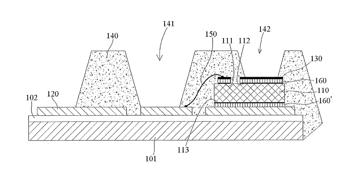
[0042]FIG. 1 is an illustrative cross section view of a power semiconductor module according to a first exemplary embodiment of the present invention.

[0043]In an embodiment of the present invention, a power semiconductor module is disclosed. As shown in FIG. 1, the power semiconductor module mainly comprises a substrate 120, a semiconductor 110 and a package 140.

[0044]As shown in FIG. 1, the semiconductor 110 is provided on a top side of the substrate 120. The package 140 is formed on the semiconductor 110 and the substrate 120. As shown in FIG. 1, the package 140 has openings 141, 142 formed therein at a top side thereof, through which terminal contacts of the semiconductor 110 and the substrate 120 are exposed outside and accessible from outside. The terminal contacts of the semiconductor 110 and the substrate 120 that are exposed outside and accessible from outside may be pressure-contacted with a printed circuit board by, for example, pressure-contact springs.

[0045]In an exempla...

second embodiment

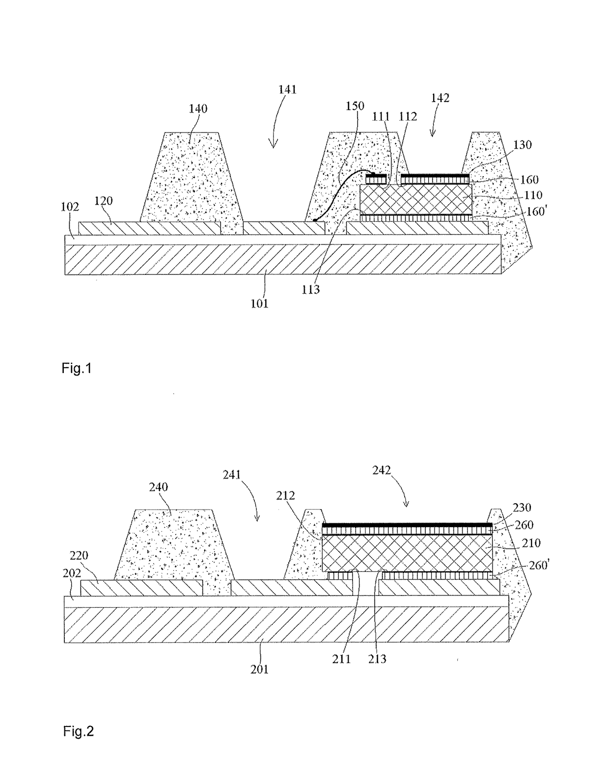
[0057]FIG. 2 is an illustrative cross section view of a power semiconductor module according to a second exemplary embodiment of the present invention.

[0058]In an embodiment of the present invention, a power semiconductor module is disclosed. As shown in FIG. 2, the power semiconductor module mainly comprises a substrate 220, a semiconductor 210 and a package 240.

[0059]As shown in FIG. 2, the semiconductor 210 is provided on a top side of the substrate 220. The package 240 is formed on the semiconductor 210 and the substrate 220. As shown in FIG. 2, the package 240 has openings 241, 242 formed therein at a top side thereof, through which terminal contacts of the semiconductor 210 and the substrate 220 are exposed outside and accessible from outside. The terminal contacts of the semiconductor 210 and the substrate 220 that are exposed outside and accessible from outside may be pressure-contacted with a printed circuit board by, for example, pressure-contact springs.

[0060]In an exempl...


PUM


Abstract

The present invention discloses a power semiconductor module, comprising: a substrate; a semiconductor provided on a top side of the substrate; and a package formed on the semiconductor and the substrate, wherein the package has openings at a top side thereof, through which terminal contacts of the semiconductor and the substrate are exposed outside and accessible from outside.

Description

CROSS-REFERENCE TO RELATED APPLICATION[0001]This application is a National Stage application of International Patent Application No. PCT / EP2016 / 065683, filed on Jul. 4, 2016, which claims priority to German Patent Application No. 10 2015 112 451.3, filed on Jul. 30, 2015, each of which is hereby incorporated by reference in its entirety.BACKGROUND OF THE INVENTIONField of the Invention[0002]The present invention relates to a power semiconductor module.Background Art[0003]The contacting of power modules and associated printed circuit boards by means of pressure contacting is known. In the case of these modules, pressure-contact springs integrated in the module or the housing cover thereof reach down to terminal areas of a DCB (Direct Copper Bond) substrate. Direct contacting of power semiconductors is not envisaged. The contact areas are initially brought into electrical contact with the terminal areas of the DCB substrate by means of wire bonding. From there, the electrical connecti...

Claims


Application Information

Patent Timeline
Patent Type & Authority Applications(United States)
IPC IPC(8): H01L23/31H01L23/00H01L23/495
CPCH01L23/3185H01L24/73H01L24/33H01L24/32H01L24/29H01L23/49544H01L24/48H01L2224/48247H01L2224/29139H01L2224/32245H01L2224/33181H01L2224/73265H01L23/142H01L24/72H01L23/3121H01L2224/04042H01L2224/06181H01L2924/15192H01L2924/1815H01L2224/32225H01L2224/48227H01L2224/0603H01L2224/48091H01L2224/05647H01L2224/05639H01L2224/03505H01L24/03H01L24/05H01L24/06H01L2924/15323H01L2224/16227H01L2224/72H01L2924/00H01L2924/00012H01L2924/00014H01L2224/29339
Inventor OSTERWALD, FRANKEISELE, RONALDULRICH, HOLGER
Owner DANFOSS SILICON POWER
Why Eureka
Try Eureka