Method of pattern placement correction

a pattern placement and pattern technology, applied in the direction of semiconductor/solid-state device testing/measurement, instruments, photomechanical equipment, etc., can solve the problems of connection misplacement in individual dies, yield loss, and limit throughput,

Active Publication Date: 2018-08-09
APPLIED MATERIALS INC
View PDF2 Cites 0 Cited by
  • Summary
  • Abstract
  • Description
  • Claims
  • Application Information

AI Technical Summary

Problems solved by technology

The placement accuracy requirement limits throughput and increase cost.
Warpage of the substrate, among other issues, can lead to connection misplacement in the individual dies.
Excessive die drift during pick-and-place operation also contribute to yield loss.
Thus, misplacing cingulated chips to form a molded panel can lead to pattern overlay difficulties in the buildup process when traditional lithography is used.

Method used


Image

  • Method of pattern placement correction
  • Method of pattern placement correction
  • Method of pattern placement correction

Examples


Embodiment Construction

[0014]The present invention includes methods and apparatus for correcting a pattern placement on a substrate during a photolithography processes. In one embodiment, the substrate is transferred to a metrology tool. The substrate is measured to determine die locations on the substrate, skew of the dies, warpage of the substrate, and other pattern mappings. The substrate is subsequently moved to a digital lithography system for processing therein. Die misplacement on the substrate is corrected by applying a per-die digital mask alignment correction. Correction for substrate warpage induced placement errors of each die is performed by applying a model based pattern placement correction algorithm based on the measurements taken from the metrology tool.

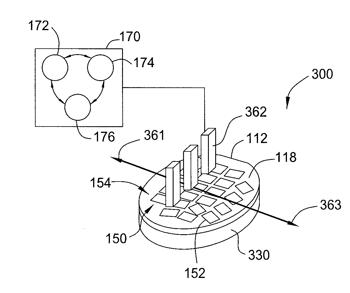
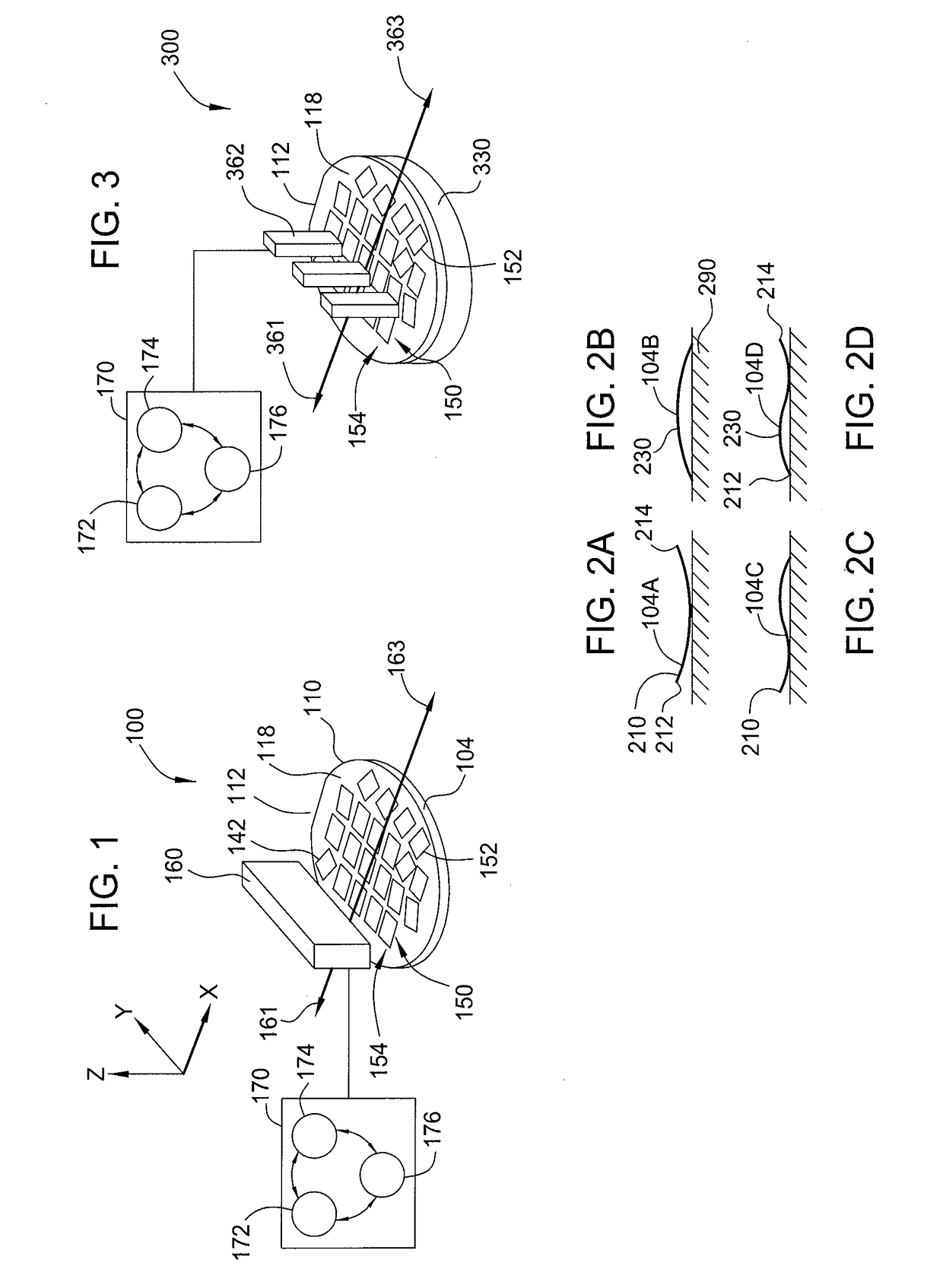
[0015]FIG. 1 is a schematic view of a substrate 104 disposed in a metrology system 100. The metrology system 100 may have a scanner 160. The scanner 160 may move in a first direction 161 and a second direction 163 to fully measure the subs...


PUM

PropertyMeasurementUnit
electricalaaaaaaaaaa
shapeaaaaaaaaaa
warpageaaaaaaaaaa

Abstract

In one embodiment of the invention, a method for correcting a pattern placement on a substrate is disclosed. The method begins by detecting three reference points for a substrate. A plurality of sets of three die location points are detected, each set indicative of an orientation of a die structure, the plurality of sets include a first set associated with a first dies and a second set associated with a second die. A local transformation is calculated for the orientation of the first die and the second on the substrate. Three orientation points are selected from the plurality of sets of three die location points wherein the orientation points are not set members of the same die. A first global orientation of the substrate is calculated from the selected three points from the set of points and the first global transformation and the local transformation for the substrate are stored.

Description

BACKGROUNDField[0001]Embodiments of the present disclosure generally relate to methods for processing one or more substrates, and more specifically to methods for performing photolithography processes.Description of the Related Art[0002]Microlithography techniques are generally employed to create electrical features incorporated as part of a die formed on a substrate. According to this technique, a light-sensitive photoresist is typically applied to a surface of the substrate. Then, a pattern generator exposes selected areas of the light-sensitive photoresist as part of a pattern with light to cause chemical changes to the photoresist in the selective areas to create a mask. The mask is utilized to transfer a pattern during the creation of the electrical features that eventually make up the die.[0003]However, as multiple operations are involved in the formation of the electrical features, high placement accuracy for masks forming the individual dies are required to align the connect...

Claims


Application Information

Patent Timeline
Patent Type & Authority Applications(United States)
IPC IPC(8): H01L23/00H01L21/66G03F7/20
CPCH01L24/02H01L22/20H01L2224/02321H01L2224/02313G03F7/70625H01L2924/37001H01L2224/96H01L2924/3511G03F7/70633G03F7/70783H01L22/12H01L2225/06596H01L2223/54453
Inventor COSKUN, TAMERCHEN, JANG FUNG
Owner APPLIED MATERIALS INC
Why Eureka
Try Eureka