Organic light emitting display device

a light-emitting display device and organic technology, applied in the field of display devices, can solve the problems of relatively small thickness, light weight, and relatively low power consumption of organic light-emitting display devices, and achieve the effects of reducing or effectively preventing damage to the organic light-emitting layer, and reducing or effectively preventing damage to the organic light-emitting elemen

Active Publication Date: 2018-08-16
SAMSUNG DISPLAY CO LTD
View PDF16 Cites 4 Cited by
  • Summary
  • Abstract
  • Description
  • Claims
  • Application Information

AI Technical Summary

Benefits of technology

[0027]The organic light emitting display device according to one or more embodiment may include the via insulation layer which may not overlap the organic light emitting layer, therefore, damage to the organic light emitting layer may be reduced or effectively prevented. The organic light emitting display device according to one or more embodiment may include the via insulation layer which may not overlap the organic light emitting element of at least one sub-pixel, therefore, damage to the organic light emitting element may be reduced or effectively prevented.

Problems solved by technology

The organic light emitting display device may not include a separate light source to generate light, and thus the organic light emitting display device may have relatively small thickness and light weight as well as relatively low power consumption.

Method used


Image

  • Organic light emitting display device
  • Organic light emitting display device
  • Organic light emitting display device

Examples


Embodiment Construction

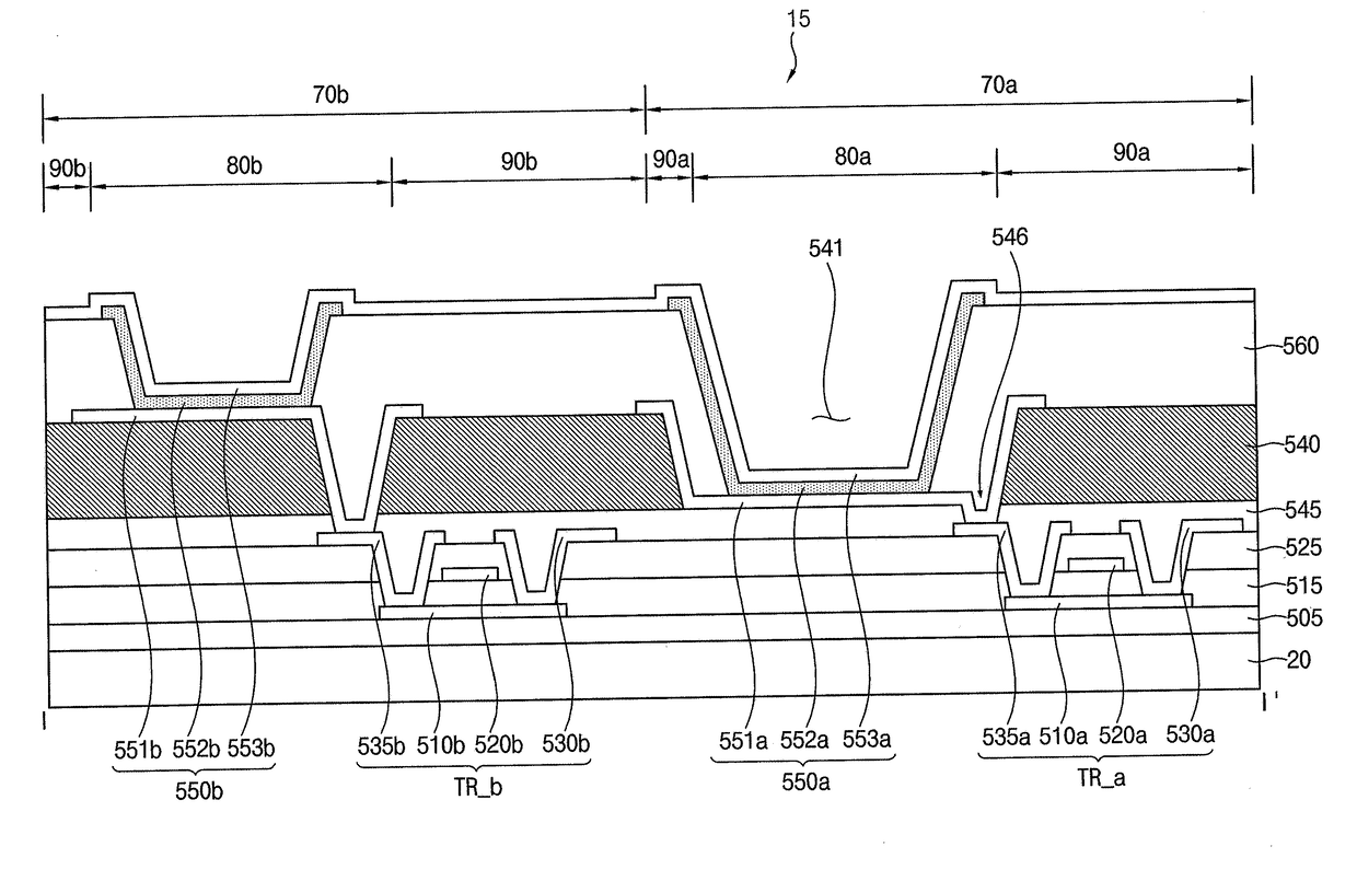
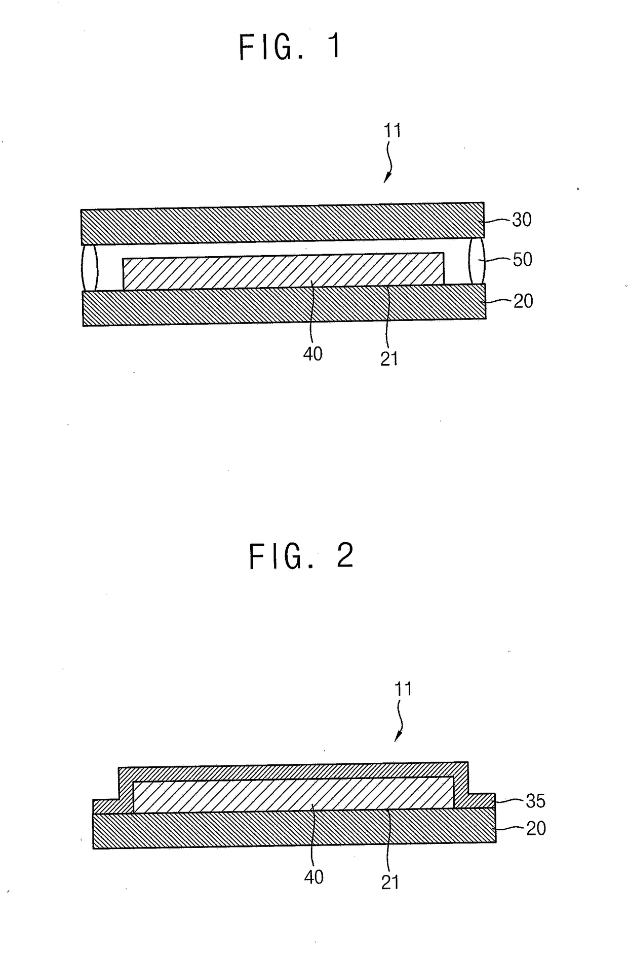
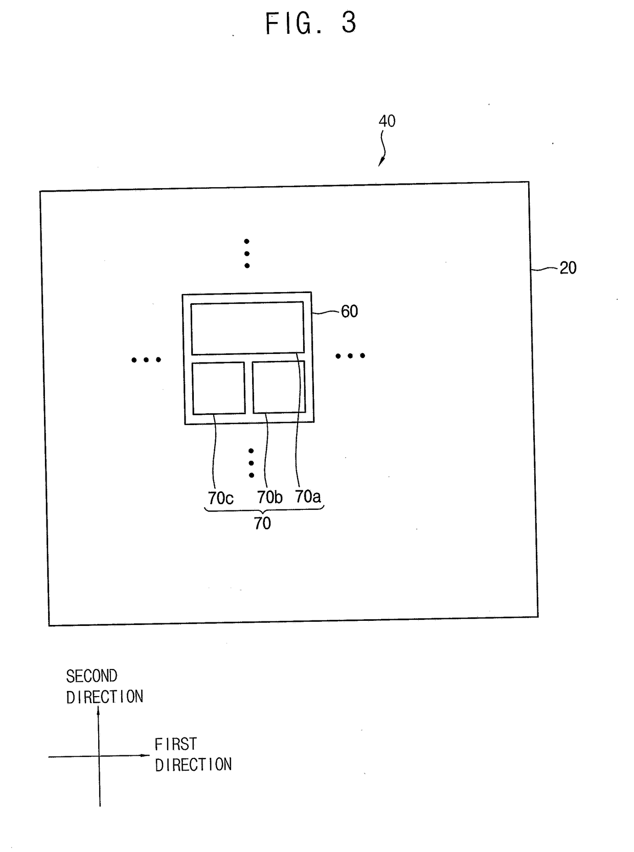
[0038]The invention now will be described more fully hereinafter with reference to the accompanying drawings, in which various embodiments are shown. This invention may, however, be embodied in many different forms, and should not be construed as limited to the embodiments set forth herein. Rather, these embodiments are provided so that this disclosure will be thorough and complete, and will fully convey the scope of the invention to those skilled in the art. Like reference numerals refer to like elements throughout.

[0039]It will be understood that when an element is referred to as being “on” another element, it can be directly on the other element or intervening elements may be present therebetween. In contrast, when an element is referred to as being “directly on” another element, there are no intervening elements present.

[0040]It will be understood that, although the terms “first,”“second,”“third” etc. may be used herein to describe various elements, components, regions, layers a...


PUM


Abstract

An organic light emitting display device includes a substrate including an emission region and a non-emission region, an organic light emitting element which emits light, the organic light emitting element including a first electrode disposed on the substrate in the emission region, an organic light emitting layer disposed on the first electrode in the emission region, and a second electrode disposed on the organic light emitting layer, and a via insulation layer disposed on the substrate in the non-emission region thereof, the via insulation layer including an organic insulation material. The via insulation layer defines an opening therein in which the organic light emitting layer of the organic light emitting element is disposed.

Description

[0001]This application claims priority to Korean Patent Application No. 10-2017-0018742, filed on Feb. 10, 2017, and all the benefits accruing therefrom under 35 U.S.C. § 119, the content of which in its entirety is herein incorporated by reference.BACKGROUND1. Field[0002]Embodiments relate to display devices. More particularly, embodiments relate to organic light emitting display devices.2. Description of the Related Art[0003]An organic light emitting display device may have an organic light emitting element including a hole injection layer, an electron injection layer, and an organic light emitting layer formed therebetween. In the organic light emitting display device, light may be generated as excitons, which are the combination of holes injected from the hole injection layer and electrons injected from the electron injection layer, fall from an excited state to a ground state.[0004]The organic light emitting display device may not include a separate light source to generate lig...

Claims


Application Information

Patent Timeline
Patent Type & Authority Applications(United States)
IPC IPC(8): H01L27/32
CPCH01L27/3246H01L27/3258H10K59/12H10K59/121H10K59/123H10K59/124H10K59/353H10K50/81H10K59/122
Inventor CHUNG, JINKOOKIM, GUNHEEKIM, KYUNGHOKIM, SEONG-MINNAM, EUNKYOUNGCHOI, CHAUNGI
Owner SAMSUNG DISPLAY CO LTD
Why Eureka
Try Eureka