

Liquid crystal display device and turning film for liquid crystal display device
a liquid crystal display and turning film technology, applied in the direction of optics, instruments, optical light guides, etc., can solve the problems of polarization-induced color and luminance irregularities, greater birefringence, and liquid crystal display devices that may be affected by polarization
- Summary
- Abstract
- Description
- Claims
- Application Information
AI Technical Summary
Benefits of technology
Problems solved by technology
Method used
Image

Examples
first embodiment
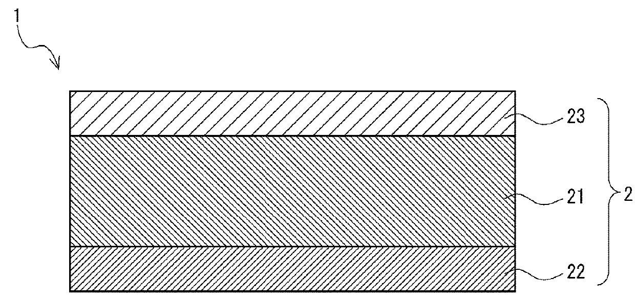
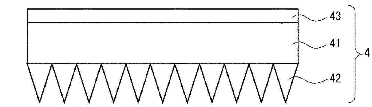
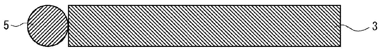
[0022]A liquid crystal display device 1 shown in FIG. 1 includes: a liquid crystal panel 2; a light-guiding plate (a light guide film 3) that is disposed on a back face side of the liquid crystal panel 2 and is for guiding rays of light incident on an end face of the light-guiding plate toward a front face side; at least one LED light source 5 disposed along the end face of the light guide film 3; and a turning film 4 disposed between the liquid crystal panel 2 and the light guide film 3. Due to the need of transmission of rays of light, the light guide film 3 and the turning film 4 are formed to be transparent. The liquid crystal display device 1 further includes a reflection plate (not shown) that is disposed on a back face side of the light guide film 3 such that rays of light incident on the reflection plate from the front face side bounce back to the front face side.
[0023]Liquid Crystal Panel
[0024]The liquid crystal panel 2 includes: a liquid crysta...
second embodiment
[0049]A liquid crystal display device 11 shown in FIG. 2 includes: the liquid crystal panel 2; the light-guiding plate (the light guide film 3) that is disposed on the back face side of the liquid crystal panel 2 and is for guiding rays of light incident on the end face of the light-guiding plate toward the front face side; the at least one LED light source 5 disposed along the end face of the light guide film 3; and the turning film 4 disposed between the liquid crystal panel 2 and the light guide film 3. The liquid crystal display device 11 further includes a bonding layer 6 disposed between the liquid crystal panel 2 and the turning film 4. The liquid crystal display device 11 may be similar to the liquid crystal display device 1 shown in FIG. 1 except that the bonding layer 6 is included. Thus, the following description will be given solely on the bonding layer 6.
[0050]Bonding Layer
[0051]The bonding layer 6 bonds the turning film 4 to another member ...
PUM
| Property | Measurement | Unit |
|---|---|---|
| refractive index | aaaaa | aaaaa |
| refractive index | aaaaa | aaaaa |
| refractive index | aaaaa | aaaaa |
Abstract
Description
Claims
Application Information