Edge structure for multiple layers of devices, and method for fabricating the same

Active Publication Date: 2018-10-11
MACRONIX INT CO LTD
View PDF2 Cites 1 Cited by
  • Summary
  • Abstract
  • Description
  • Claims
  • Application Information

AI Technical Summary

Benefits of technology

This patent describes a way to reduce wasted space in a chip by designing an edge structure for multiple layers of devices. By adjusting the elevation angle of the second stair structure, the width of the stair area in the second direction is made smaller, resulting in less waste of chip area. Overall, this invention provides a more efficient and effective solution for designing complex integrated circuits.

Problems solved by technology

However, since the contact plugs and the patterns of Metal 1 are formed over the area of the X-directional (or Y-directional) staircase only, most of the area of the Y-directional (or X-directional) stair is wasted.

Method used


Image

  • Edge structure for multiple layers of devices, and method for fabricating the same
  • Edge structure for multiple layers of devices, and method for fabricating the same
  • Edge structure for multiple layers of devices, and method for fabricating the same

Examples


Embodiment Construction

[0021]This invention is further explained with the following embodiments, which are just exemplary but are not intended to limit the scope of this invention.

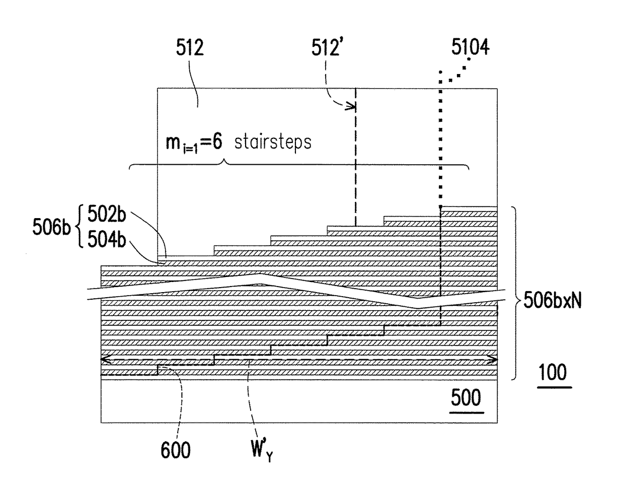
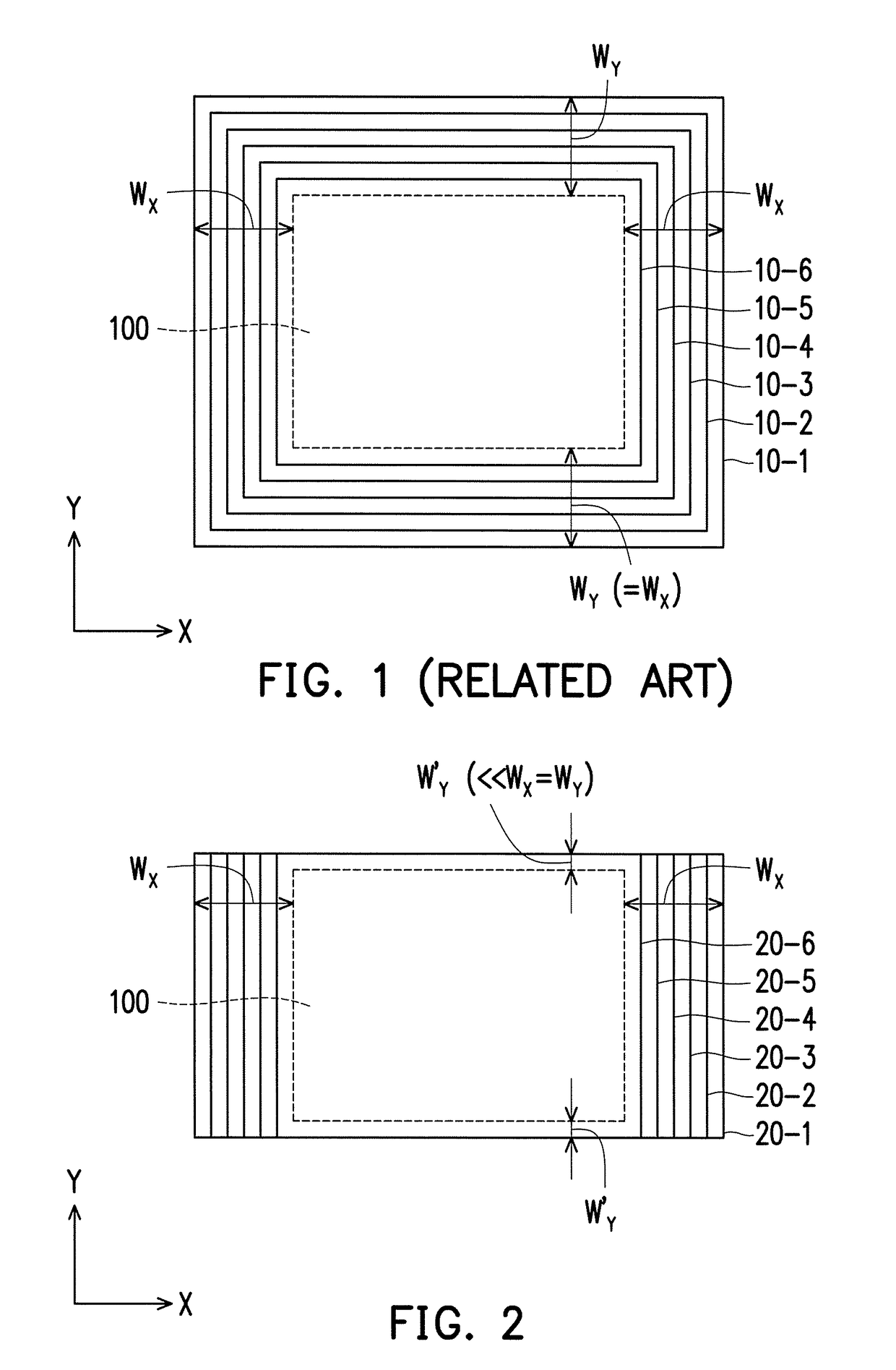
[0022]FIG. 2 illustrates a mask design for fabricating an edge structure for multiple layers of devices according to an embodiment of this invention. The multiple layers of devices may comprise a 3D memory array.

[0023]Referring to FIG. 2, in this embodiment, six mask layers 20-1, 20-2, 20-3, 20-4, 20-5 and 20-6 are formed in sequence at different time points, and the direction at which contacts for the multiple layers of devices are to be formed is X-direction. The firstly formed mask layer 20-1 defines the borders of both the X-directional stair structure and the Y-directional stair structure, wherein the distance between the X-directional border of the mask layer 20-1 and the area 100 of the multiple layers of devices is namely the width WX of the X-directional stair structure to be formed, and the distance between the Y-direc...


PUM


Abstract

An edge structure for multiple layers of devices including stacked multiple unit layers includes first and second stair structures. The first stair structure is at a first direction of the devices where device contacts are formed, including first edge portions of the unit layers at the first direction, of which the borders gradually retreat with increase of level height. The elevation angle from the border of the first edge portion of the bottom unit layer to that of the top one is a first angle. The second stair structure includes second edge portions of the unit layers at a second direction. The variation of border position of the second edge portion with increase of level height is irregular. The elevation angle from the border of the second edge portion of the bottom unit layer to that of the top one is a second angle larger than the first angle.

Description

BACKGROUND OF THE INVENTIONField of Invention[0001]This invention relates to a structure applicable to integrated circuits and fabrication thereof, and particularly relates to an edge structure for multiple layers of devices, and a method for fabricating the same.Description of Related Art[0002]In a structure of multiple layers of devices, such a three-dimensional (3D) device array such as a 3D memory array, the conductive lines for the respective levels of devices require electrical connection, so the conductive layers of the respective levels have to be exposed in a contact area for later electrical connection. As a result, a staircase contact pad structure is formed.[0003]In a conventional method, such a stair structure is formed around the area of multiple layers of devices by forming a series of mask layers that gradually decrease in size and performing a plurality of one-layer etching steps and a plurality of mask trimming steps alternately between the respective formation ste...

Claims


Application Information

Patent Timeline
IPC IPC(8): H01L23/528H01L27/105H01L23/532H01L21/311H01L21/768H01L21/02
CPCH01L23/5283H01L27/1052H01L23/53295H01L21/02164H01L21/76895H01L21/0217H01L21/31144H10B43/50
Inventor YANG, CHIN-CHENG
Owner MACRONIX INT CO LTD
Why Eureka
Try Eureka