
Optical modeling method and electronic apparatus using the same

a technology of optical modeling and electronic equipment, applied in the field of optical modeling method for building lens models and electronic equipment, can solve the problems of wasting a lot of time in the current design method, and achieve the effect of saving the time for designing the lens

Inactive Publication Date: 2018-10-18
LITE ON ELECTRONICS (GUANGZHOU) LTD +1
View PDF0 Cites 1 Cited by
  • Summary
  • Abstract
  • Description
  • Claims
  • Application Information

AI Technical Summary

Benefits of technology

The invention provides an optical modeling method and an electronic apparatus that can quickly build a lens model and accurately produce a light shape close to the desired target. This saves time and effort in the lens design process. The method involves calculating the lens model based on the first target intensity distribution, the external shape of the light source, and the spatial intensity distribution of the light source. The lens model is then repeatedly adjusted based on the difference between the first intensity distribution and the first target intensity distribution, resulting in a final target lens model that is close to the target intensity distribution. This allows the light source to generate a light shape close to the desired target shape.

Problems solved by technology

However, the current designing method takes a lot of time because the light distribution curve of the lens is unpredictable.

Method used


Image

  • Optical modeling method and electronic apparatus using the same
  • Optical modeling method and electronic apparatus using the same
  • Optical modeling method and electronic apparatus using the same

Examples


Embodiment Construction

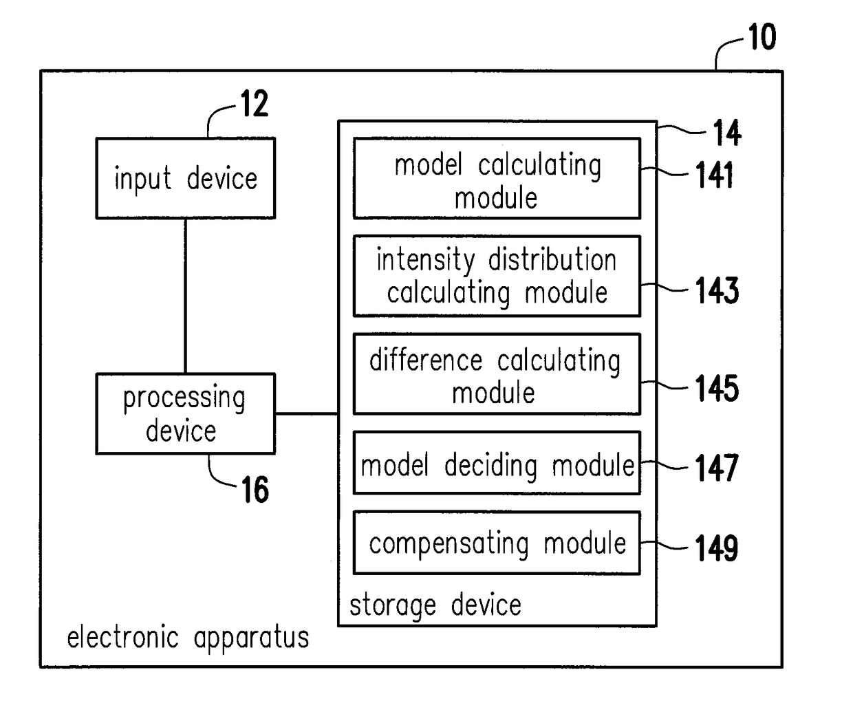
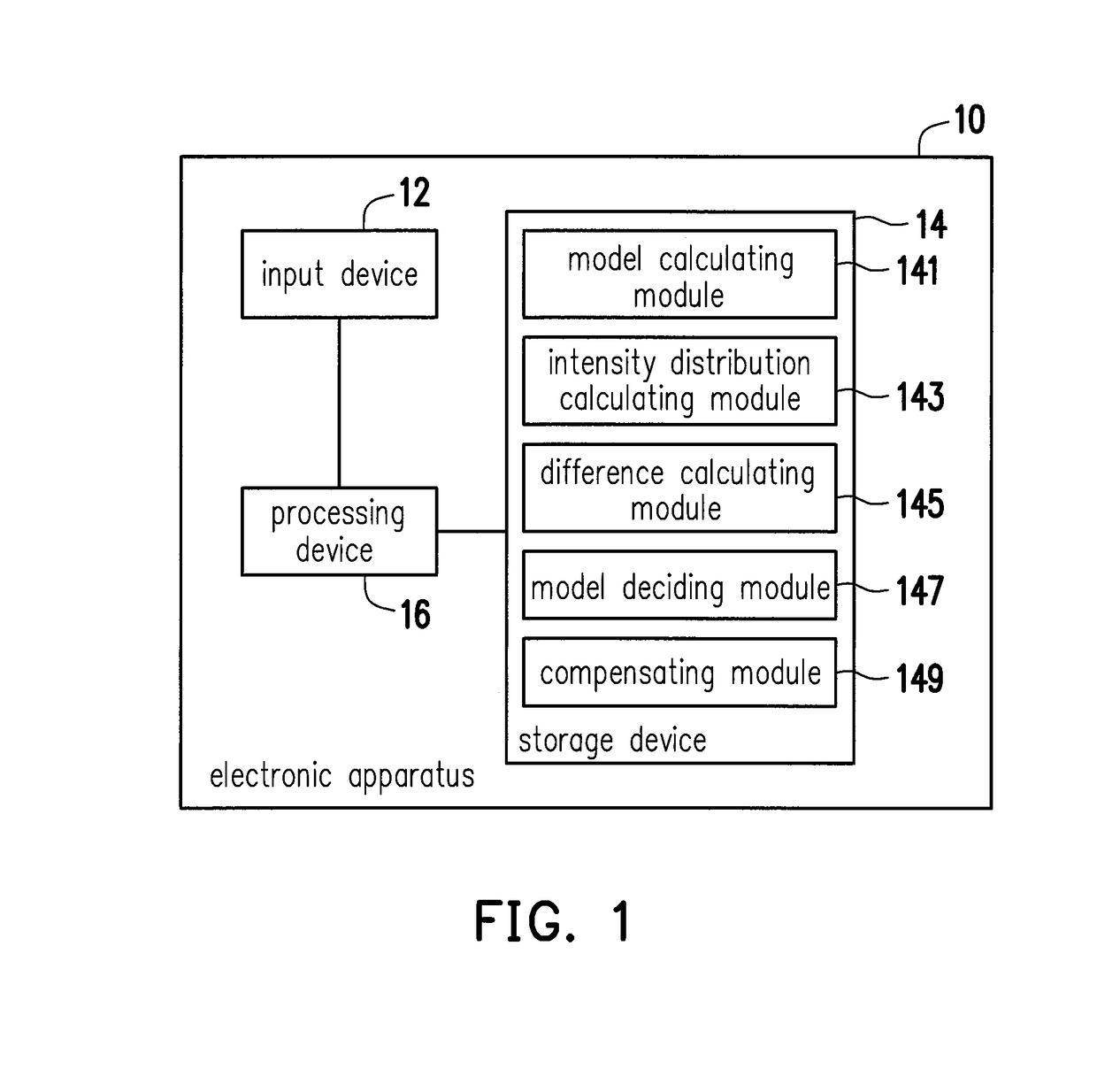
[0018]FIG. 1 is a schematic block diagram of an electronic apparatus according to an embodiment of the invention. An electronic apparatus 10 of this embodiment is configured to build a target lens model for a light source to generate a light shape or intensity distribution that is close to an expected target intensity distribution after light of the light source passes the target lens model. In this embodiment, the electronic apparatus 10 is, for example, a personal computer, a mobile phone, a tablet computer, a server, or other apparatuses having an operational function, which includes at least an input device 12, a storage device 14, and a processing device 16. Functions of each of these devices are described as follows:

[0019]The input device 12 is a keyboard, a mouse, etc., for example, configured to receive an input signal. In this embodiment, the input signal received by the input device 12 includes, for example, a first target intensity distribution. The first target intensity...


PUM


Abstract

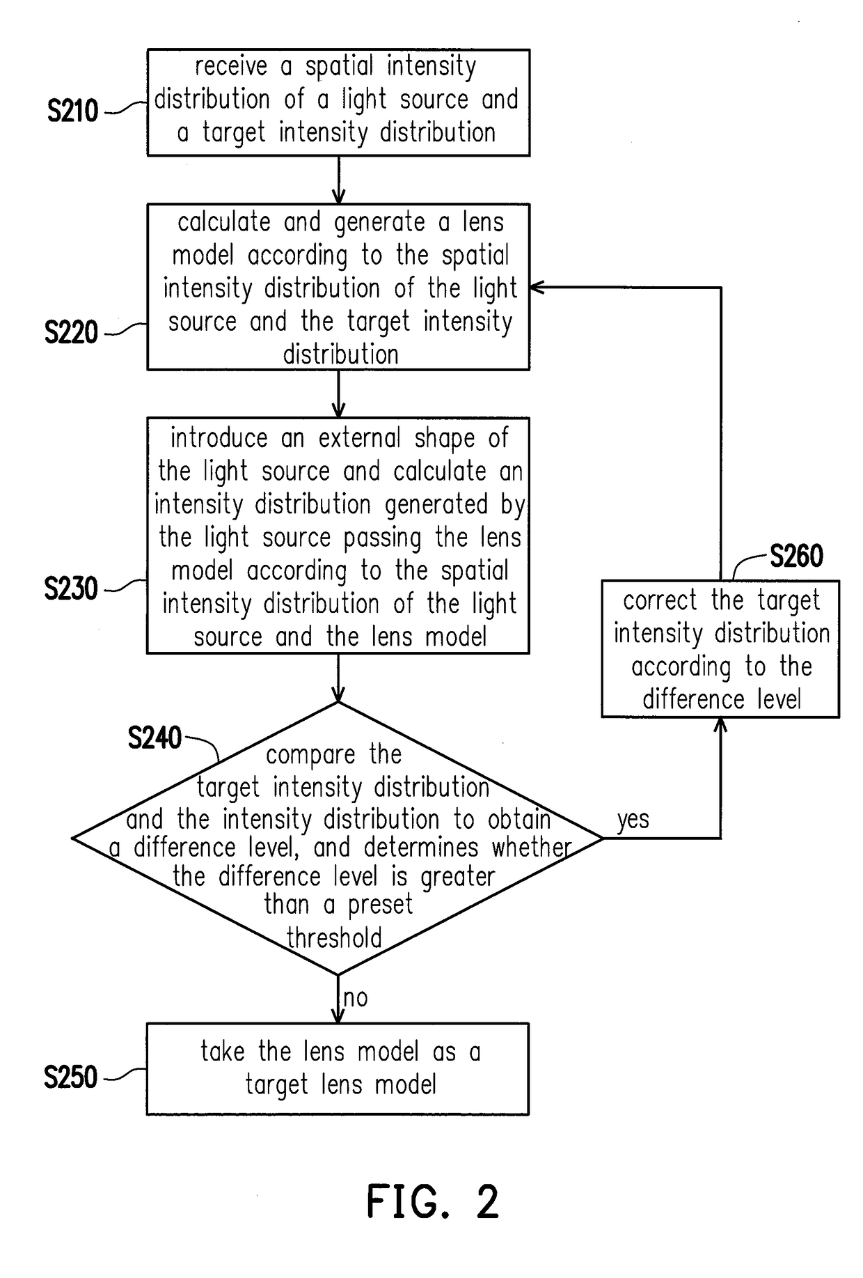
An optical modeling method and an electronic apparatus for building a target lens model are provided. The optical modeling method includes: calculating and generating a first lens model according to a spatial intensity distribution of a light source and a first target intensity distribution; introducing an external shape of the light source and calculating a first intensity distribution according to the spatial intensity distribution and the first lens model; obtaining a first difference level by comparing the first target intensity distribution and the first intensity distribution; taking the first lens model as the target lens model if the first difference level is not greater than preset threshold; otherwise, correcting the first target intensity distribution to a second target intensity distribution according to the first difference level, and calculating and generating a second lens model according to the spatial intensity distribution of the light source and the second target intensity distribution.

Description

CROSS-REFERENCE TO RELATED APPLICATION[0001]This application claims the priority benefit of Taiwan application serial no. 106112921, filed on Apr. 18, 2017. The entirety of the above-mentioned patent application is hereby incorporated by reference herein and made a part of this specification.BACKGROUND OF THE INVENTION1. Field of the Invention[0002]The invention relates to a modeling method, and particularly relates to an optical modeling method for building a lens model and an electronic apparatus using the optical modeling method.2. Description of Related Art[0003]In recent years, as the improvement of luminous efficiency and lifetime of light emitting diode (LED), along with the component features and advantages thereof, such as low power consumption, low pollution, high-efficiency, high speed of response, small volume, light weight, and installability on various kinds of surfaces, LED has been positively applied in various optical fields. Take the use of. LED on illumination for...

Claims


Application Information

Patent Timeline
IPC IPC(8): G02B27/00G02B27/09F21V5/04
CPCG02B27/0012G02B27/0955F21V5/04G02B27/0927G02B19/0009G02B3/08G02B19/0061
Inventor WANG, SHIH-CHANGSHIH, WEI-WENHSU, PIN-HAO
Owner LITE ON ELECTRONICS (GUANGZHOU) LTD
Learn More