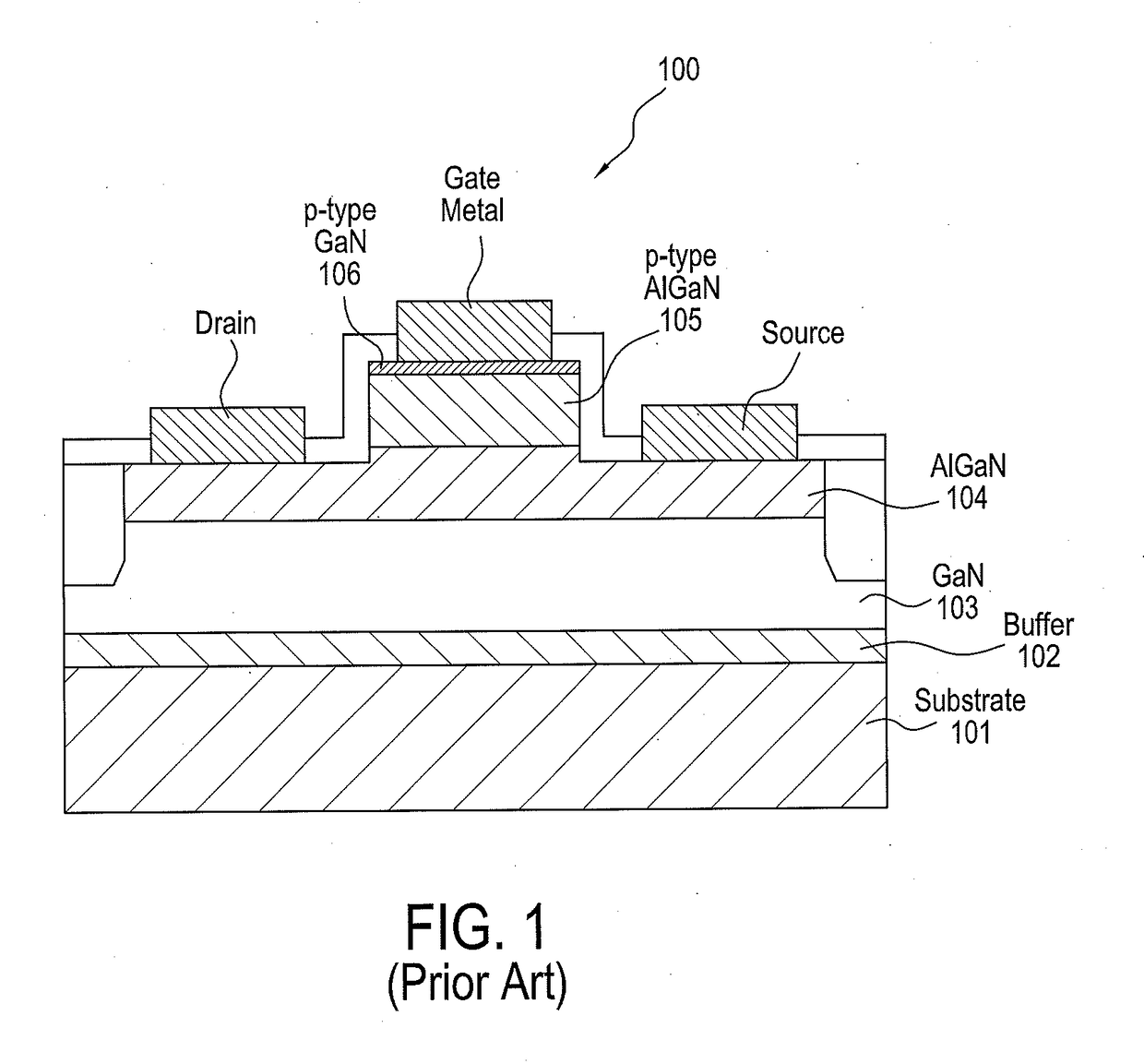
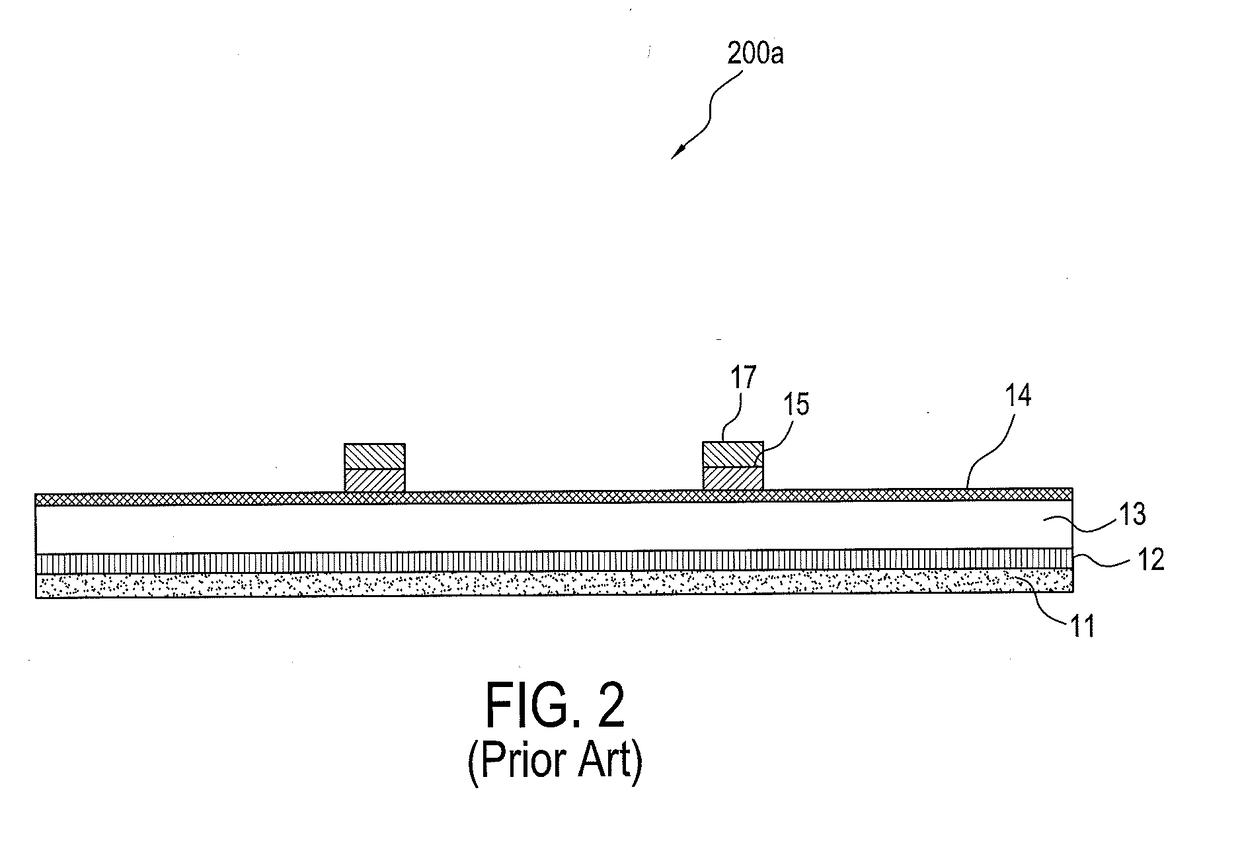
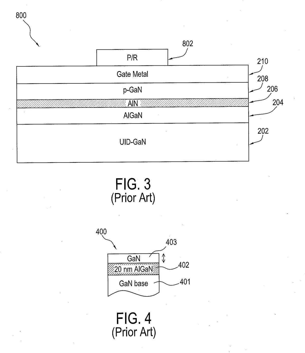
ENHANCEMENT-MODE GaN TRANSISTOR WITH SELECTIVE AND NONSELECTIVE ETCH LAYERS FOR IMPROVED UNIFORMITY IN GaN SPACER THICKNESS

a technology of gan spacer layer and enhancement mode, which is applied in the direction of basic electric elements, electrical equipment, semiconductor devices, etc., can solve the problem that the device/fet b>400/b> is only operable, and achieve the effect of improving the uniformity of the gan spacer layer and minimizing or eliminating the damage to the barrier layer

Active Publication Date: 2018-12-20
EFFICIENT POWER CONVERSION CORP
View PDF3 Cites 5 Cited by
  • Summary
  • Abstract
  • Description
  • Claims
  • Application Information

AI Technical Summary

Benefits of technology

The present invention provides an enhancement-mode transistor gate structure that includes an etch stop layer near the front barrier layer to improve the uniformity and thickness of the GaN spacer layer during manufacturing. This results in improved performance and reliability of the transistor structure.

Problems solved by technology

However, device / FET 400 is only operable for depletion mode HEMT FETs.

Method used


Image

  • ENHANCEMENT-MODE GaN TRANSISTOR  WITH SELECTIVE AND NONSELECTIVE ETCH LAYERS FOR IMPROVED UNIFORMITY IN GaN SPACER THICKNESS
  • ENHANCEMENT-MODE GaN TRANSISTOR  WITH SELECTIVE AND NONSELECTIVE ETCH LAYERS FOR IMPROVED UNIFORMITY IN GaN SPACER THICKNESS
  • ENHANCEMENT-MODE GaN TRANSISTOR  WITH SELECTIVE AND NONSELECTIVE ETCH LAYERS FOR IMPROVED UNIFORMITY IN GaN SPACER THICKNESS

Examples


first embodiment

[0029]FIG. 5 illustrates a cross-sectional view of an enhancement-mode transistor structure 500 formed according to the present invention. As shown in the embodiment of FIG. 5, the present invention is directed to an enhancement-mode transistor gate structure 500, comprising: an AlGaN front barrier layer 504; a GaN spacer layer 505 disposed above the barrier layer, a p-GaN layer 506 disposed above GaN layer 505; a pAlGaN etch stop layer 507 disposed above the p-GaN layer 506, and a pGaN layer 508 disposed above pAlGaN etch stop layer 507. The barrier layer 504 may comprise one or more barrier layers.

[0030]In a preferred embodiment, the pAlGaN etch stop layer 507 has a thickness of 0.5 nm to 2 nm. The pGaN layer 506 has a thickness of 1 nm to 30 nm, and is thinner than the pGaN layer 508, which has a thickness of 20 nm to 100 nm. The GaN gate spacer layer 505 has a thickness of 1 nm to 6 nm, and is thicker below the etch stop layer 507 than in surrounding areas.

[0031]The gate spacer ...

sixth embodiment

[0040]FIG. 13 illustrates a cross-sectional view of an enhancement-mode transistor structure 1300 formed according to the present invention. In the embodiment of FIG. 13, the transistor gate structure 1300 comprises additional pAlGaN (or pAlInGaN) etch stop layers 527 and 547 and an additional pGaN layer 510 disposed between pAlGaN (or pAlInGaN) etch stop layers 527 and 547. A gate metal 560 is disposed above the top pAlGaN (or pAlInGaN) etch stop layer 547. FIG. 13 also illustrates ohmic contact metals 502, 503 on either side of the barrier layer 504 and are spaced from the gate region. A GaN channel layer 501 is positioned below the barrier layer 504.

[0041]As in the prior embodiment, a pAlGaN (or pAlInGaN) etch stop layer 507 is located near the AlGaN barrier layer, where dimension a508 above the etch stop layer 507 and the material 506 below the etch stop layer 507 may be pGaN, pAlGaN, or pAlInGaN, and their Al content (if present) is less than the Al content in the etch stop lay...


PUM


Abstract

An enhancement-mode transistor gate structure which includes a spacer layer of GaN disposed above a barrier layer, a first layer of pGaN above the spacer layer, an etch stop layer of p-type Al-containing column III-V material, for example, pAlGaN or pAlInGaN, disposed above the first p-GaN layer, and a second p-GaN layer, having a greater thickness than the first p-GaN layer, disposed over the etch stop layer. The etch stop layer minimizes damage to the underlying barrier layer during gate etching steps, and improves GaN spacer thickness uniformity.

Description

CROSS REFERENCE TO RELATED APPLICATIONS[0001]This application claims priority from U.S. Provisional Application No. 62 / 520,262, filed on Jun. 15, 2017, the disclosure of which is hereby incorporated herein by reference in its entirety.FIELD OF THE INVENTION[0002]The present invention relates to the field of enhancement-mode transistor structures such as gallium nitride (GaN) transistor structures. More particularly, the invention relates to GaN transistor gate structures with an etch stop p-type Al-containing column III-V material layer of, for example, pAlGaN or pAlInGaN, positioned above at least one spacer layer of, for example, pGaN.BACKGROUND OF THE INVENTION[0003]Gallium nitride (GaN) semiconductor devices are increasingly desirable for power semiconductor devices because of their ability to carry large current and support high voltages. Development of these devices has generally been aimed at high power / high frequency applications. Devices fabricated for these types of applic...

Claims


Application Information

Patent Timeline
Patent Type & Authority Applications(United States)
IPC IPC(8): H01L29/66H01L21/306H01L29/43H01L29/778
CPCH01L29/66462H01L21/30621H01L29/432H01L29/7787H01L29/41766H01L29/7786H01L29/1066H01L29/2003H01L21/28587H01L27/0605
Inventor CAO, JIANJUNBEACH, ROBERTZHAO, GUANGYUANSARIPALLI, YOGANANDTANG, ZHIKAI
Owner EFFICIENT POWER CONVERSION CORP
Why Eureka
Try Eureka