

Light receiving device, method of manufacturing light receiving device, imaging device, and electronic apparatus
- Summary
- Abstract
- Description
- Claims
- Application Information
AI Technical Summary
Benefits of technology
Problems solved by technology
Method used
Image

Examples
embodiment
[Configuration]
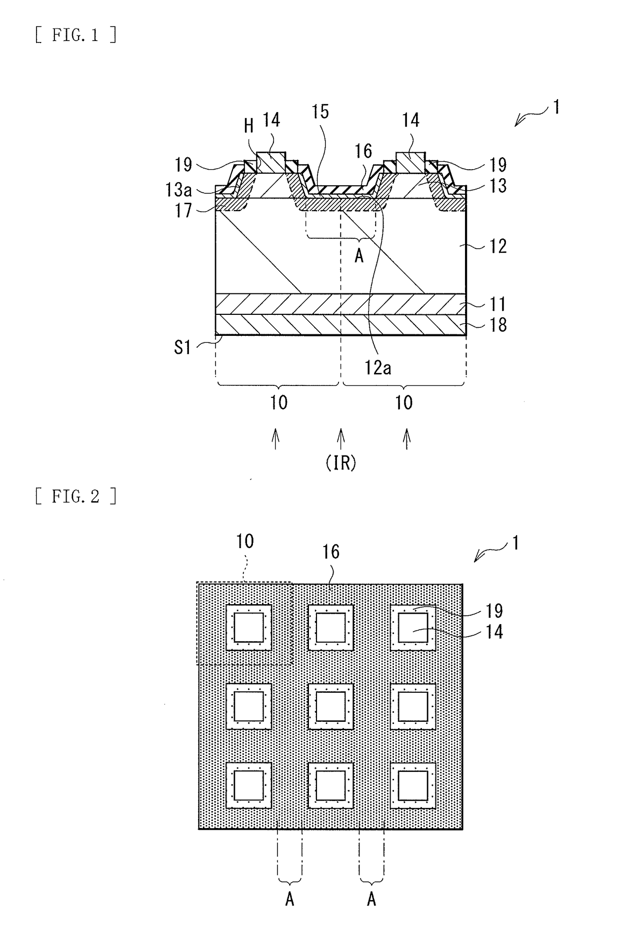
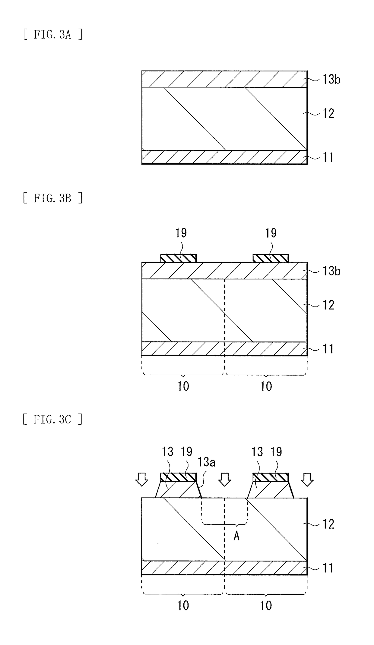
[0048]FIG. 1 illustrates a cross-sectional configuration of a light receiving device (a light receiving device 1) according to an embodiment of the present disclosure. FIG. 2 illustrates a planar configuration of the light receiving device 1 in a schematic manner. The light receiving device 1 is applicable to, for example, an infrared sensor, etc. using a compound semiconductor, and includes pixels 10 (corresponding to pixels P of an imaging device as described later) serving as a plurality of light receiving unit regions that are disposed two-dimensionally, for example. It is to be noted that FIG. 1 illustrates the cross-sectional configuration of a portion corresponding to two pixels P.
[0049]The light receiving device 1 includes, for example, a photoelectric conversion layer 12 and a plurality of contact layers 13 in this order on a substrate 11. An electrode (a first electrode 14) is electrically coupled to each of the plurality of contact layers 13. A covering lay...
modification example 1
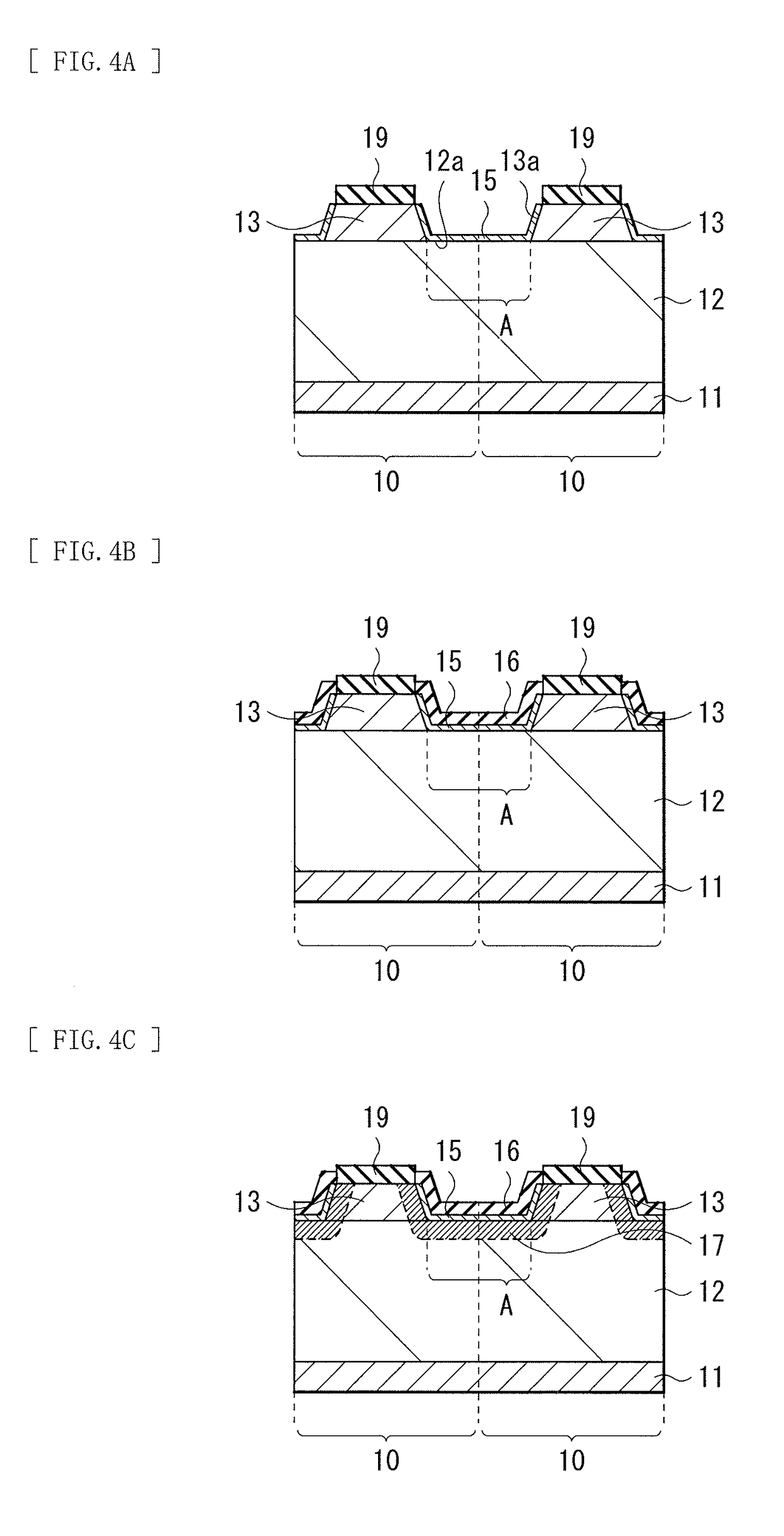
[0086]FIG. 9 illustrates a cross-sectional configuration of a light receiving device (a light receiving device 1A) according to a modification example 1. As with the above-described embodiment, the light receiving device 1A includes, for example, the photoelectric conversion layer 12 and the plurality of contact layers 13 in this order on the substrate 11, and the plurality of contact layers 13 are provided on the photoelectric conversion layer 12 at the spacing intervals A with respect to one another. The first electrode 14 is electrically coupled to each of the plurality of contact layers 13 through the opening H of the mask layer 19. A covering layer (a covering layer 15A) and insulating films (insulating films 16A and 16) are formed in this order to cover a portion (the surface 12a) of the front surface of the photoelectric conversion layer 12 and the side surface 13a of each of the contact layers 13. A diffusion region (a diffusion region 17A) including an impurity is formed in...
modification example 2
[0090]FIG. 10 illustrates a cross-sectional configuration of a light receiving device (a light receiving device 1B) according to a modification example 2. As with the above-described embodiment, the light receiving device 1B includes, for example, the photoelectric conversion layer 12 and the plurality of contact layers 13 in this order on the substrate 11, and the plurality of contact layers 13 are provided on the photoelectric conversion layer 12 at the spacing intervals A with respect to one another. The first electrode 14 is electrically coupled to each of the plurality of contact layers 13 through the opening H of the mask layer 19. A covering layer (a covering layer 15B) and the insulating film 16 are formed in this order to cover a portion (the surface 12a) of the front surface of the photoelectric conversion layer 12 and the side surface 13a of each of the contact layers 13. A diffusion region (a diffusion region 17B) including an impurity is formed in a region adjacent to t...
PUM
 Abstract
Description
Claims
Application Information