Assembly of semiconductor devices

a technology for semiconductor devices and led dies, applied in semiconductor devices, semiconductor/solid-state device testing/measurement, instruments, etc., can solve the problems of complex second placement cycle, if not impossible, and achieve the effect of high throughput and fine resolution to manipula

Active Publication Date: 2019-01-24
META PLATFORMS TECH LLC
View PDF4 Cites 13 Cited by
  • Summary
  • Abstract
  • Description
  • Claims
  • Application Information

AI Technical Summary

Benefits of technology

[0059]Exemplary methods disclosed herein may have a fine resolution to manipulate and handle small dies and may achieve a high throughput. This may enable, for example, massive parallel pick and transfer of ILED dies of sizes <10 μm a side from the native LED wafer onto a glass TFT substrate at accuracies approx ±2 μm or less.
[0060]In exemplary methods disclosed herein a deformable material (forming an intermediate layer) may be deposited on a surface of one or more ILED dies, and a head of a non-conformal pick-up tool (PUT) may be used to contact the deposited deformable material. The upper surface of the intermediate layer contacts the PUT and may cause the ILED dies to adhere to the PUT head through the intermediate layer. The PUT, with a plurality of ILED dies adhered to its head, may direct the chips to a desired position over a glass or plastics thin film transistor panel substrate. Then, the upper surface of intermediate layer may be released from the PUT head so that the intermediate layer and ILED dies remain appropriately located on the receiving substrate. The PUT may be non-conformable. The intermediate layer may be deformable such that it is able to make conformal contact with the ILED dies. The intermediate layer on the ILED dies may enable selection of particular ILED dies, such as selection between defective ILED dies and KGD.

Problems solved by technology

This makes the second placement cycle much more complicated, if not impossible.

Method used


Image

  • Assembly of semiconductor devices
  • Assembly of semiconductor devices
  • Assembly of semiconductor devices

Examples


Embodiment Construction

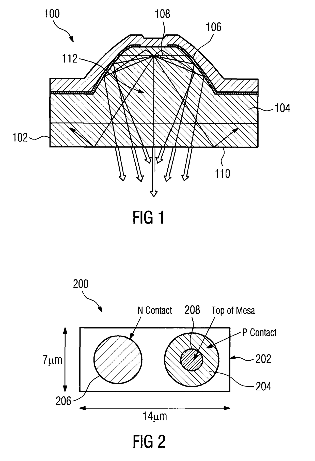
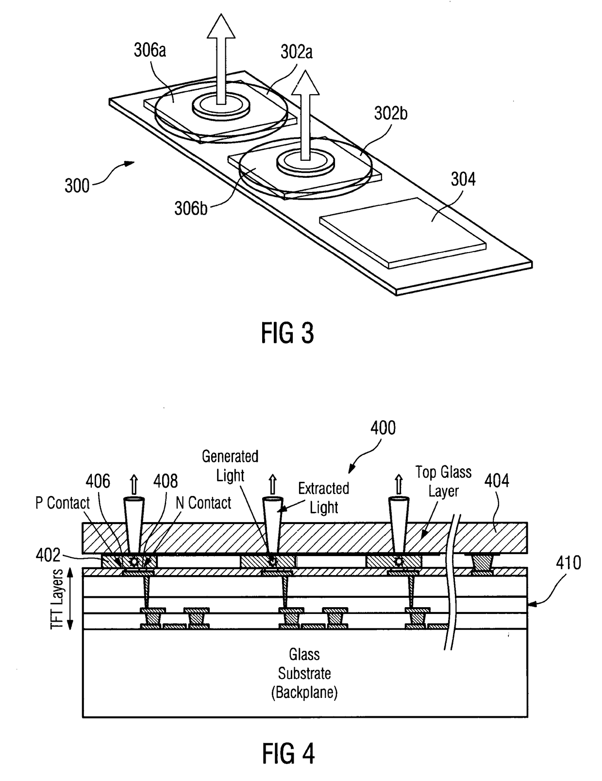
[0166]The inventors have appreciated that ILED Displays may provide future generations of flat display image generators providing superior battery performance and enhanced brightness. The ILED Display is at a basic level a variation of the OLEO display. The OLEO concept is based on passing current through organic or polymer materials that are sandwiched between two glass planes to produce light.

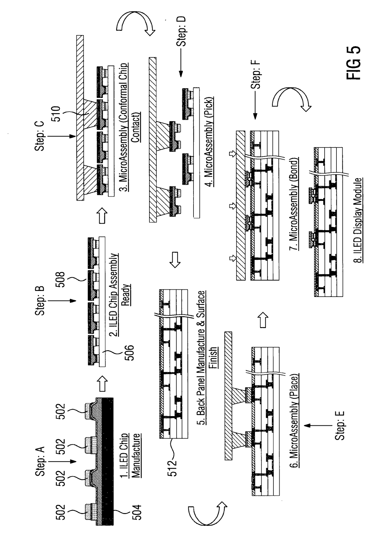
[0167]ILED display manufacture refers to the assembly of semiconductor inorganic light emitting diode (ILED) or other microLED devices onto flexible substrates or substrates such as TFT glass substrates. The assembly of millions of small μLEDs chips to create an ILED display can create unique challenges, for example, when considering wafer and assembly yield losses and the test strategy during in-line assembly onto non-native substrates.

[0168]The inventors have further appreciated some challenges with ILED display manufacture, as set out below.

[0169]High LED wafer yields greater than or equal...


PUM


Abstract

A method for manufacturing a display element comprising a plurality of pixels, each comprising a plurality of sub-pixels. The method comprises undertaking, using a pick up tool, a first placement cycle (1908) comprising picking up a plurality of first, untested LED dies and placing them on a display substrate at locations corresponding to the plurality of pixels, testing (1912) the first LED emitters on the display substrate to determine one or more locations of non-functional first LED emitters, selecting one or more second tested LED dies based on a result of the test, configuring the selected one or more second LED dies to enable their pick up and placement on the display substrate and undertaking, using the PUT, a second placement cycle (2008) comprising picking up the selected one or more second LED dies and placing them on the display substrate at the determined locations of the non-functional first LED emitters.

Description

CROSS REFERENCE TO RELATED APPLICATIONS[0001]This application is a National Phase application of International Application No. PCT / GB2016 / 052722, filed Apr. 11, 2016, which claims the benefit of United Kingdom Application No. 20150006486.8, filed Sep. 2, 2016, which claims the benefit of United Kingdom Application No. 1515564.1, filed Sep. 2, 2015, United Kingdom Application No. 201520265.8, filed Nov. 17, 2015, United Kingdom Application No. 201607248.0, filed Apr. 26, 2016, and United Kingdom Application No. 201609422.9, filed May 27, 2016, each incorporated by reference in its entiretyTECHNICAL FIELD[0002]The invention relates to methods and apparatus for assembling semiconductor devices, LED dies for display technologies, displays and methods of manufacture for displays. Specifically, the invention is related to, but need not be limited to, Inorganic Light Emitting Diode (ILED), micro-LED (pLED) dies for display technologies, pLED displays and / or methods of manufacture for pLED ...

Claims


Application Information

Patent Timeline
Patent Type & Authority Applications(United States)
IPC IPC(8): G09G3/00H01L25/075G09G3/3225H01L33/00
CPCG09G3/006H01L25/0753G09G3/3225H01L33/0079H01L33/0095G09G2330/08H01L2224/16221H01L2224/81001H01L33/0093H01L2224/16225H01L25/075H01L27/156H01L33/20H10K59/12H01L21/683H01L22/22H01L21/563
Inventor HUGHES, PADRAIGO'KEEFFE, JOSEPHOYER, CELINEHENRY, WILLIAMMASSOUBRE, DAVIDSAKETI, POOYA
Owner META PLATFORMS TECH LLC
Why Eureka
Try Eureka