

Schottky diode
- Summary
- Abstract
- Description
- Claims
- Application Information
AI Technical Summary
Benefits of technology
Problems solved by technology
Method used
Image

Examples
first embodiment
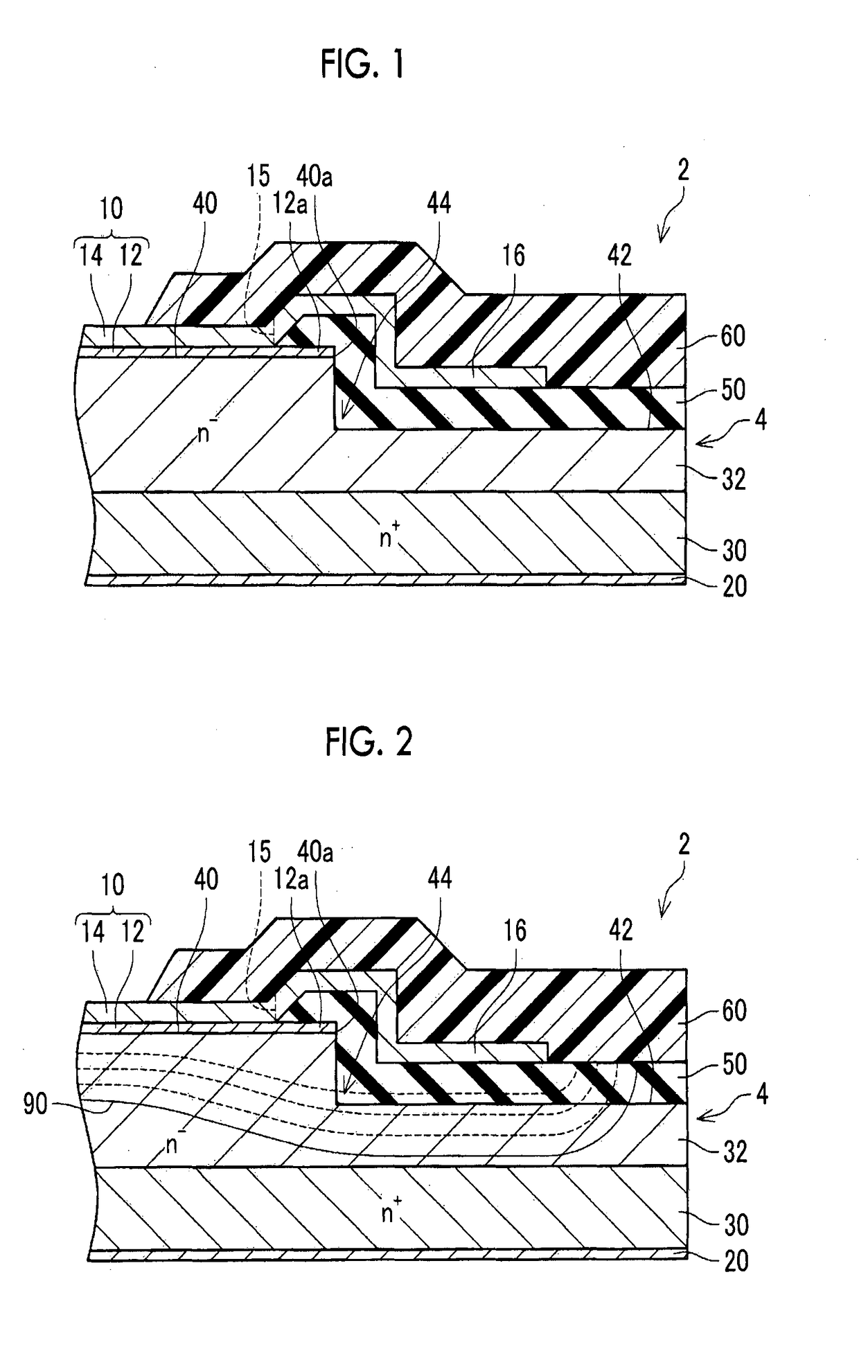
[0029]As shown in FIG. 1, the SBD 2 according to the present embodiment of the invention has a semiconductor substrate 4, an upper surface electrode 10, a field plate electrode 16, an interlayer insulating film 50, a protection film 60 and a lower surface electrode 20.
[0030]The semiconductor substrate 4 is a n-type semiconductor substrate that is formed of Ga2O3. The semiconductor substrate 4 has a lower layer 30 having a high concentration of n-type impurities, and an upper layer 32 having a lower concentration of n-type impurities than the lower layer 30. The upper layer 32 is layered on the lower layer 30. The concentration of impurities mentioned herein means an average concentration of impurities in each of the layers. The upper layer 32 functions as a drift layer of the SBD 2. An upper surface of the upper layer 32 is exposed to an upper surface of the semiconductor substrate 4, and a lower surface of the lower layer 30 is exposed to a lower surface of the semiconductor substr...
second embodiment
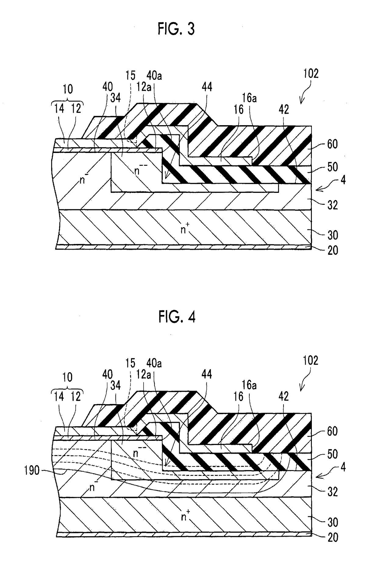
[0042]Subsequently, the SBD 102 according to the second embodiment of the invention will be described with reference to FIGS. 3 and 4, focusing on what is different from the first embodiment of the invention. In FIGS. 3 and 4, elements identical or similar to those of the SBD 2 according to the first embodiment of the invention are denoted by the same reference symbols respectively, and detailed description thereof will be omitted. The SBD 102 according to the present embodiment of the invention is different from the SBD according to the first embodiment of the invention in that a high-resistance region 34 is formed in the upper layer 32.
[0043]The high-resistance region 34 is an n-type region that is formed on the upper surface side of the upper layer 32 in a range from the end portion 40a of the first range 40 to the second range 42 via the step 44. In the present embodiment of the invention, a lower surface of the high-resistance region 34 is spaced apart from the lower layer 30. ...
third embodiment
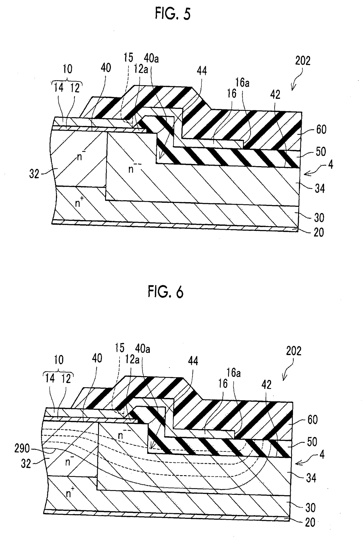
[0045]Subsequently, the SBD 202 according to the third embodiment of the invention will be described with reference to FIGS. 5 and 6, focusing on what is different from the second embodiment of the invention. In FIGS. 5 and 6, elements identical or similar to those of the SBD 2 or 102 according to each of the aforementioned embodiments of the invention are denoted by the same reference symbols respectively, and detailed description thereof will be omitted. The SBD 202 according to the present embodiment of the invention is different from the SBD according to the second embodiment of the invention in that the lower surface of the high-resistance region 34 reaches the lower layer 30, that the high-resistance region 34 reaches a lateral surface of the semiconductor substrate 4, and that the end portion 12a of the Schottky electrode film 12 is arranged at a position spaced apart from the end portion 40a of the first range 40. It should be noted herein that the lateral surface of the sem...
PUM
 Abstract
Description
Claims
Application Information