Active illumination source and PCB components having mountings for reduced z-height and improved thermal conductivity

a technology of active illumination source and pcb components, which is applied in the direction of lighting and heating apparatus, semiconductor devices for light sources, television systems, etc., can solve the problems of reducing thickness, reducing and generating a lot of heat in leds, so as to improve the thermal conductivity of pcb components and assemblies, and reduce the z height dimensions

Active Publication Date: 2019-02-21
MICROSOFT TECH LICENSING LLC
View PDF7 Cites 11 Cited by
  • Summary
  • Abstract
  • Description
  • Claims
  • Application Information

AI Technical Summary

Benefits of technology

[0007]Disclosed embodiments include PCBs, PCB components and PCB assemblies having mounting configurations and structures for

Problems solved by technology

One of the constraints associated with reducing the thickness of a mobile device is the overall profile of the integrated PCB (printed circuit board) assembly and the other components that are mounted to the PCB.
Some PCB components, such a

Method used


Image

  • Active illumination source and PCB components having mountings for reduced z-height and improved thermal conductivity
  • Active illumination source and PCB components having mountings for reduced z-height and improved thermal conductivity
  • Active illumination source and PCB components having mountings for reduced z-height and improved thermal conductivity

Examples


Embodiment Construction

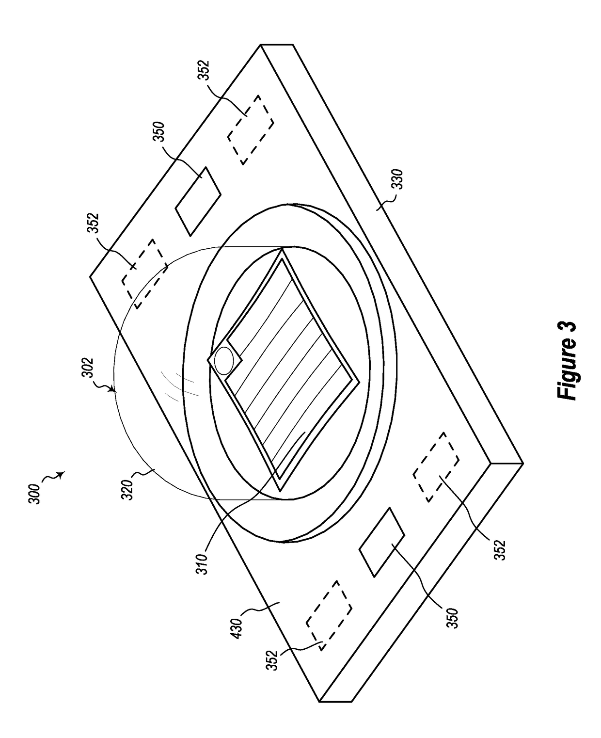
[0026]Disclosed and claimed embodiments include PCBs, PCB components and PCB assemblies having mounting configurations and structures for reducing Z height dimensions of the PCB assemblies and, in some instances, for improving thermal conductivity of the same. This is accomplished, in some instances, by providing LED devices, camera modules and other PCB components with mounting substrates having exposed elements for directly mounting the substrates to the bottom surface of a PCB, while concurrently positioning a portion of the LED device(s), camera modules or other PCB components in the hole(s) formed into the body of the PCB.

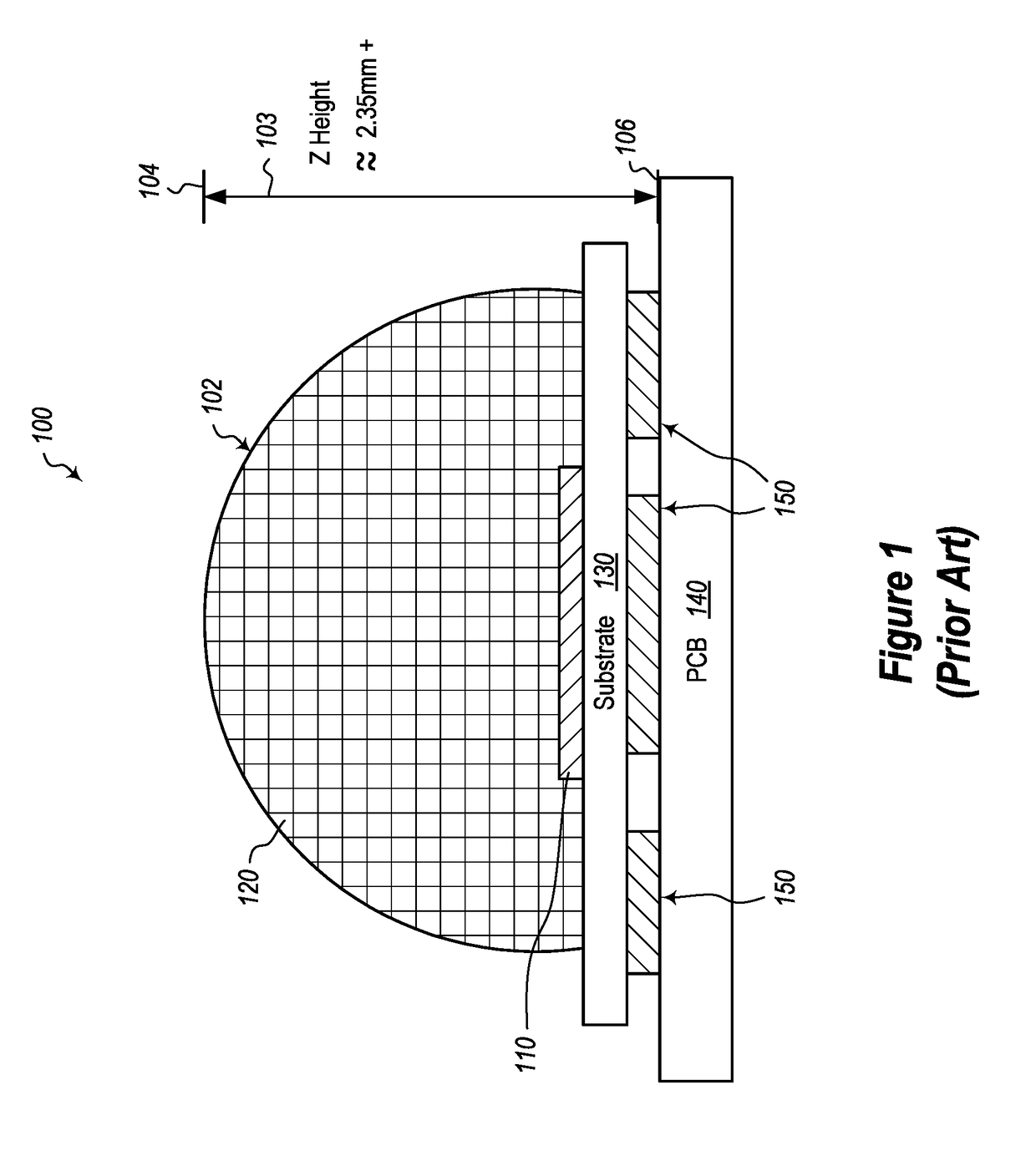
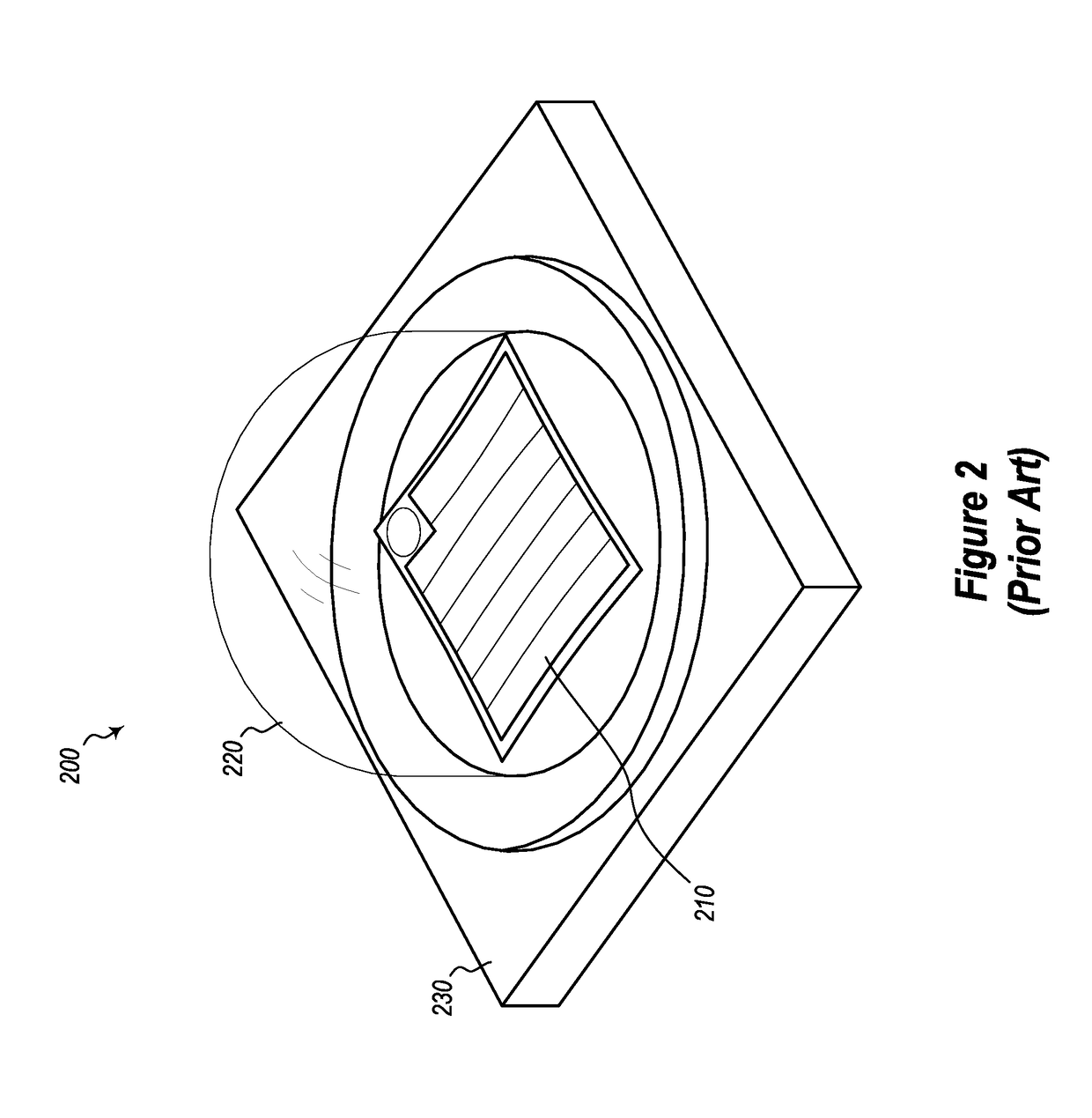
[0027]Attention will first be directed to FIGS. 1 and 2, which illustrate existing PCB assemblies and LED illuminators. In FIG. 1, discussed earlier, a typical prior art LED illuminator 100 is mounted to a top surface of a PCB. FIG. 2 illustrates another embodiment of a prior art LED illuminator 200 having a light emitting element 210 covered by a lens 220 and...


PUM


Abstract

PCBs, PCB components and PCB assemblies are provided with mounting configurations and structures for reducing Z height dimensions of the PCB assemblies and, in some instances, for improving thermal conductivity of the PCB components and assemblies. The active illumination device or other PCB components (e.g., camera modules and LED packages) are affixed to a mounting substrate that has a top surface that is physically and electrically mounted to a bottom surface of a PCB, with at least a portion of the active illumination device being concurrently positioned within one or more holes in the PCB. A thermal interface in contact with at least the mounting substrate can also be used for dissipating heat from the PCB components and PCB.

Description

BACKGROUND[0001]An ongoing focus in the mobile device industry is to design equipment that is lighter and smaller. Another focus is to increase the resolution and size of integrated display screens. Accordingly, it is most desirable to reduce a device's thickness, as the width and height of the device will limit the size of the integrated display screen.[0002]One of the constraints associated with reducing the thickness of a mobile device is the overall profile of the integrated PCB (printed circuit board) assembly and the other components that are mounted to the PCB. For instance, many PCB assemblies are configured with camera modules and active light illumination sources, such as LED (light emitting diode) illuminators, that have lenses that protrude away from the PCB.[0003]LED illuminators are typically affixed to a mounting substrate that is separately mounted to the PCB with solder, an epoxy and / or another connector. The height dimension existing between the top surface of the ...

Claims


Application Information

Patent Timeline
IPC IPC(8): F21K9/20H01L33/48H01L33/64F21V29/70H04N5/225
CPCF21K9/20H01L33/486H04N5/2257F21V29/70H01L33/64H01L33/54H01L33/62H04N23/56H04N23/57
Inventor PRICE, RAYMOND KIRKMCMILLAN, CHRISTOPHER JOHNPETERS, RACHEL LEIGH
Owner MICROSOFT TECH LICENSING LLC
Why Eureka
Try Eureka