Method of manufacturing NANO metal grating and NANO metal grating manufactured thereby
a nano metal grating and manufacturing method technology, applied in the field of display technology, can solve the problems of inability to complete etching and difficulty in ensuring that the remaining imprint glue is removed,
- Summary
- Abstract
- Description
- Claims
- Application Information
AI Technical Summary
Problems solved by technology
Method used
Image

Examples
Embodiment Construction
[0029]The preferred embodiments adopted by this disclosure are given in the following detailed description, with reference to the drawings.
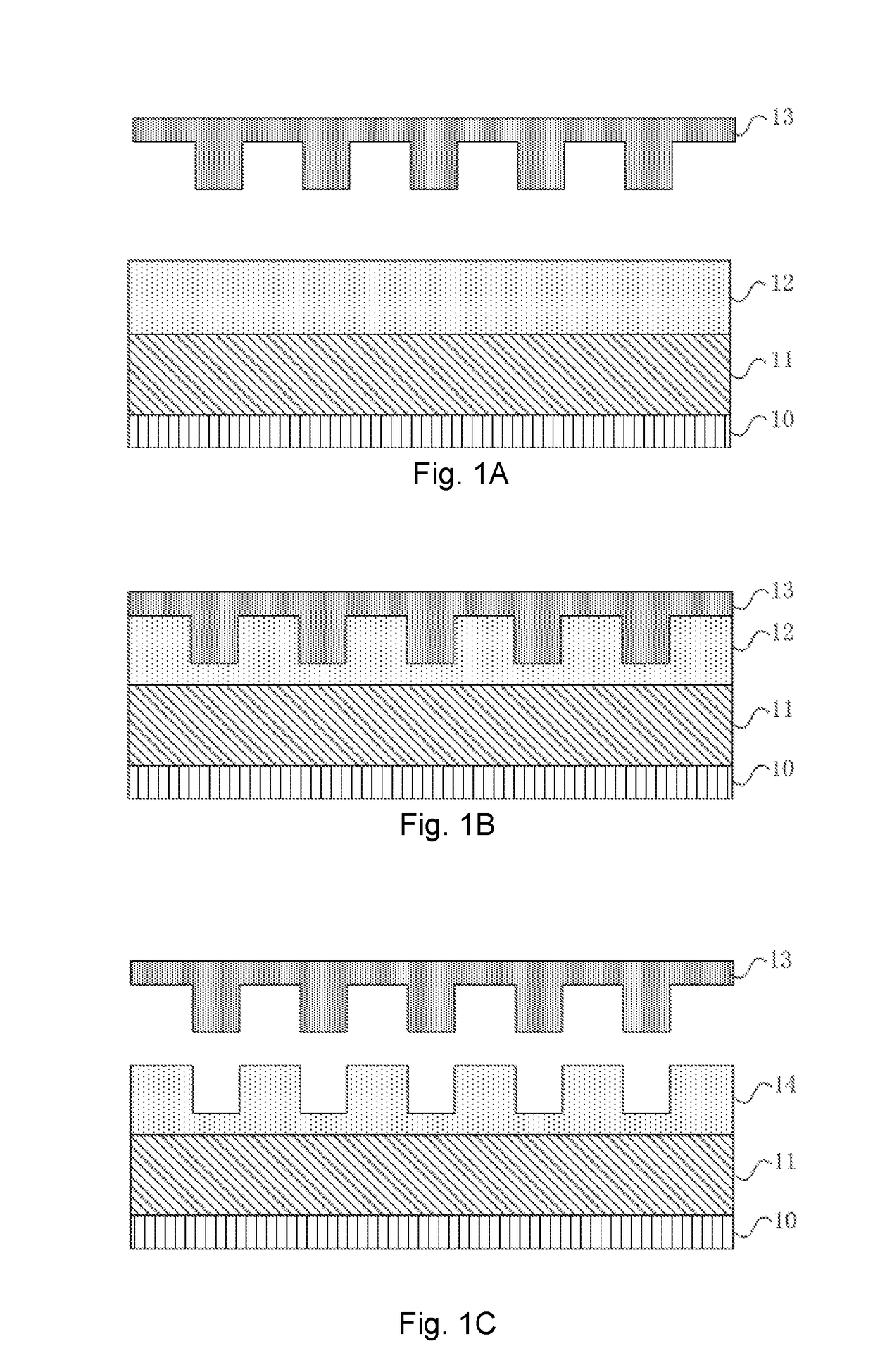
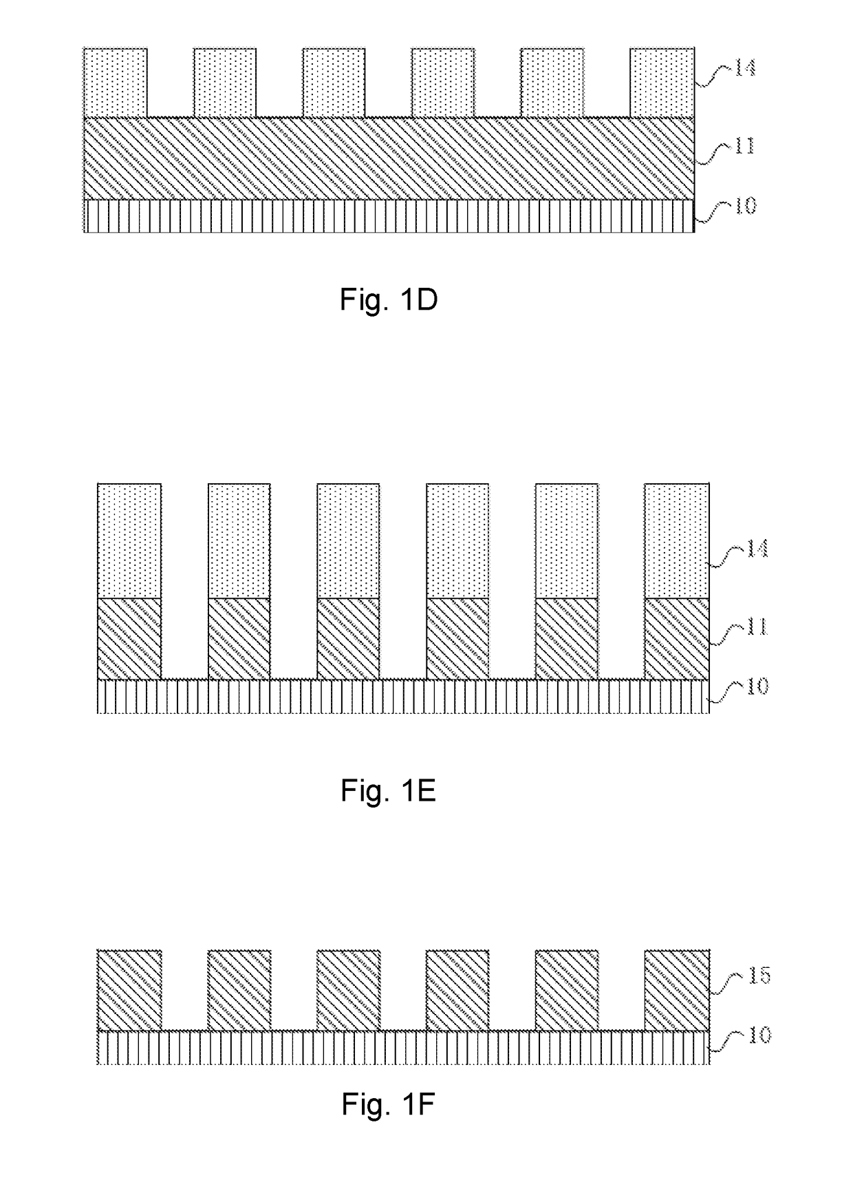
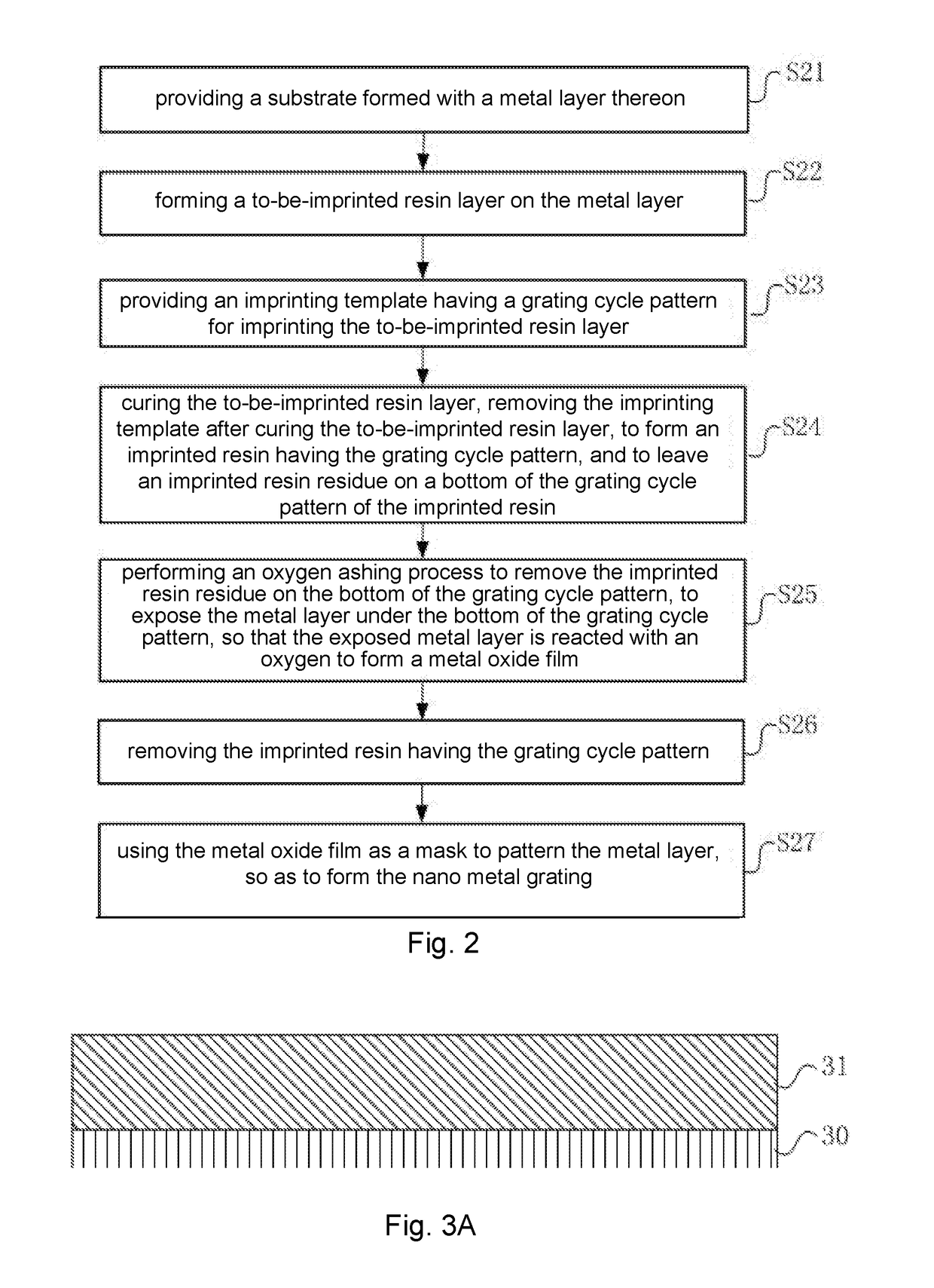
[0030]As mentioned in the background of the invention, after the remaining imprint glue is removed by the oxygen ashing method, If a processing time of the method is slightly longer or an airflow control is not accurate, oxygen will react with Al exposed on the bottom to form a dense metal oxide film. The metal oxide film is difficult to be etched, which leads to a subsequent etching step cannot be performed and is unable to form a nano-metal grating. In view of this, this disclosure provides a method of manufacturing a nano metal grating. During a step of removing remaining imprinted glue, a process time is increased so that oxygen reacts with the exposed metal to form a dense oxide film, and the oxide film is used as a barrier layer for subsequent metal etching step to form a nano-metal grating.
[0031]FIG. 2 is a step schematic of a method of ma...
PUM
| Property | Measurement | Unit |
|---|---|---|
| temperature | aaaaa | aaaaa |
| electric field | aaaaa | aaaaa |
| transmittance | aaaaa | aaaaa |
Abstract
Description
Claims
Application Information
 - R&D Engineer
- R&D Manager
- IP Professional
- Industry Leading Data Capabilities
- Powerful AI technology
- Patent DNA Extraction
Browse by: Latest US Patents, China's latest patents, Technical Efficacy Thesaurus, Application Domain, Technology Topic.
© 2024 PatSnap. All rights reserved.Legal|Privacy policy|Modern Slavery Act Transparency Statement|Sitemap