Mask plate for vapor deposition of organic light-emitting diode (OLED) devices and OLED device thereof

Active Publication Date: 2019-03-14
SHENZHEN CHINA STAR OPTOELECTRONICS SEMICON DISPLAY TECH CO LTD
View PDF2 Cites 3 Cited by
  • Summary
  • Abstract
  • Description
  • Claims
  • Application Information

AI Technical Summary

Benefits of technology

[0005]The present invention provides a mask plate for vapor deposition of organic light-emitting diode (OLED) device and an OLED device manufactured thereby that prevent organic material deposited in advance from blocking a connection hole and a

Problems solved by technology

Primary technology of large-sized white OLED (WOLED) devices is Bottom-OLED technology, designs of the Bottom-OLED technology have low aperture ratios and cannot satisfy high resolution requirements in the market.
However, because they are limited by manufacturing equipment and process, each layer of a WOLED and the cathode employ an open mask to form an entire surface of coating, issues o

Method used


Image

  • Mask plate for vapor deposition of organic light-emitting diode (OLED) devices and OLED device thereof
  • Mask plate for vapor deposition of organic light-emitting diode (OLED) devices and OLED device thereof

Examples


Example

[0044]Each of the following embodiments is described with appending figures to illustrate specific embodiments of the present invention that are applicable. The terminologies of direction mentioned in the present invention, such as “upper”, “lower”, “front”, “rear”, “left”, “right”, “inner”, “outer”, “side surface” and etc., only refer to the directions of the appended figures. Therefore, the terminologies of direction are used for explanation and comprehension of the present invention, instead of limiting the present invention. In the figures, units with similar structures are marked with the same reference numerals.

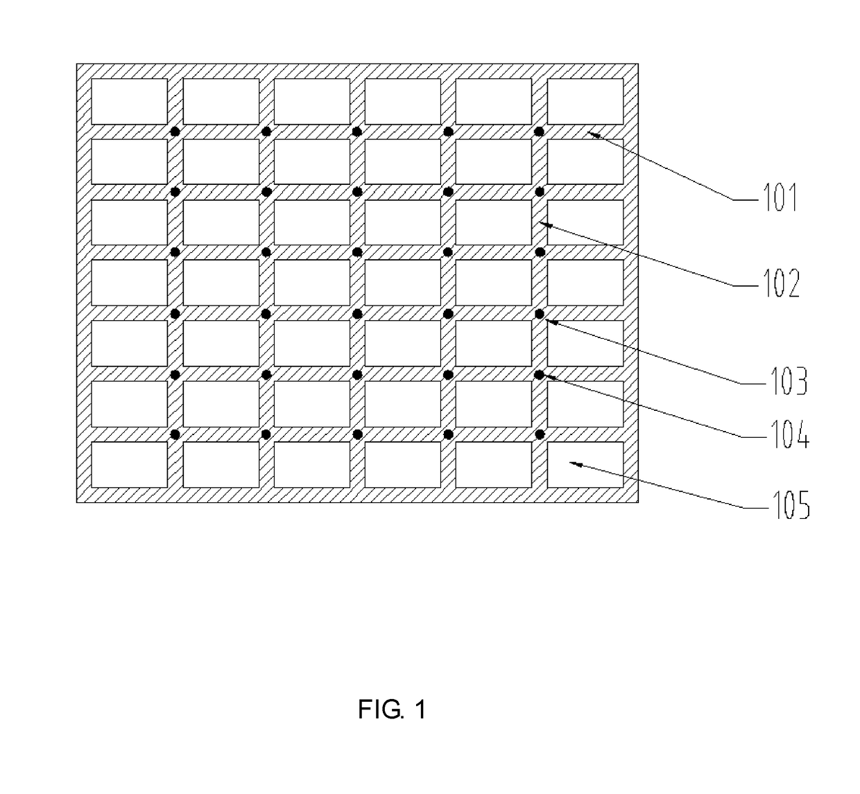
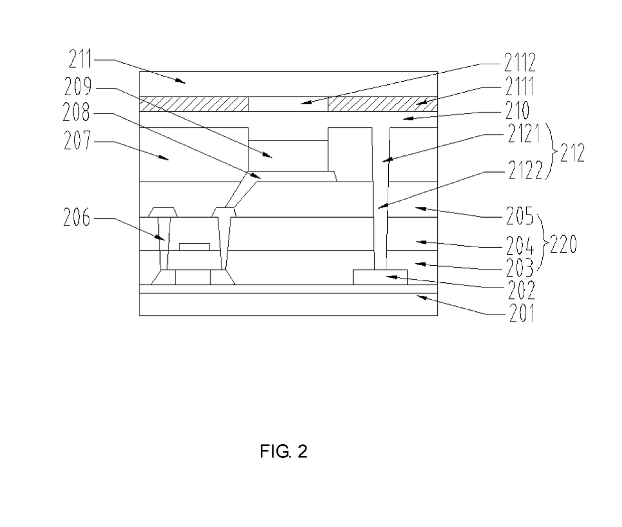
[0045]The present invention aims at issues of a conventional organic light-emitting diode (OLED) device in which organic material deposited in advance blocks a connection hole, prevents a cathode from connecting to an auxiliary cathode and thus influences voltage sag of the electrode and displaying uniformness of the display panel to affect performance of the OLED devic...


PUM

PropertyMeasurementUnit
Diameteraaaaaaaaaa
Diameteraaaaaaaaaa
Widthaaaaaaaaaa

Abstract

A mask plate for vapor deposition of an organ light-emitting diode (OLED) device and an OLED device manufactured thereby are provided. The mask plate has first slot-type mask portions disposed at intervals along a predetermined direction; second slot-type mask portions disposed at intervals along a direction perpendicular to the first slot-type mask portion and pixel regions into at least two displaying regions with the first slot-type mask portion. An intersection portion formed by the first slot-type mask portion and the second slot-type mask portion covers a connection hole connected to an auxiliary cathode.

Description

FIELD OF THE INVENTION[0001]The present invention relates to fields of displaying technologies, especially to a mask plate for vapor deposition of organic light-emitting diode (OLED) devices and an OLED device manufactured thereby.BACKGROUND OF THE INVENTION[0002]Organic light-emitting diode (OLED) display panels have advantages of low power consumption, small dimension, thinness, wide viewing angles, etc., are extensively used, and are recognized as superior display devices of next generation industries. OLED display applications in the terminal TV markets will be widespread as time passes.[0003]Primary technology of large-sized white OLED (WOLED) devices is Bottom-OLED technology, designs of the Bottom-OLED technology have low aperture ratios and cannot satisfy high resolution requirements in the market. Therefore, a Top-OLED technology for WOLEDs has been developed. Designs of the Top-OLED technology have advantages such as high resolution, excellent optical effect by transparent...

Claims


Application Information

Patent Timeline
IPC IPC(8): H01L51/00H01L27/32H01L51/52H01L51/56C23C14/04
CPCH01L51/0011H01L27/3246H01L51/001H01L51/5228H01L51/56C23C14/042H10K71/166H10K50/824H10K59/122H10K71/00H10K71/164
Inventor WEI, FENGJIANG, LIANGLI, JINCHUAN
Owner SHENZHEN CHINA STAR OPTOELECTRONICS SEMICON DISPLAY TECH CO LTD
Why Eureka
Try Eureka