

Array substrate, preparation method thereof and display device
- Summary
- Abstract
- Description
- Claims
- Application Information
AI Technical Summary
Benefits of technology
Problems solved by technology
Method used
Image

Examples
Embodiment Construction
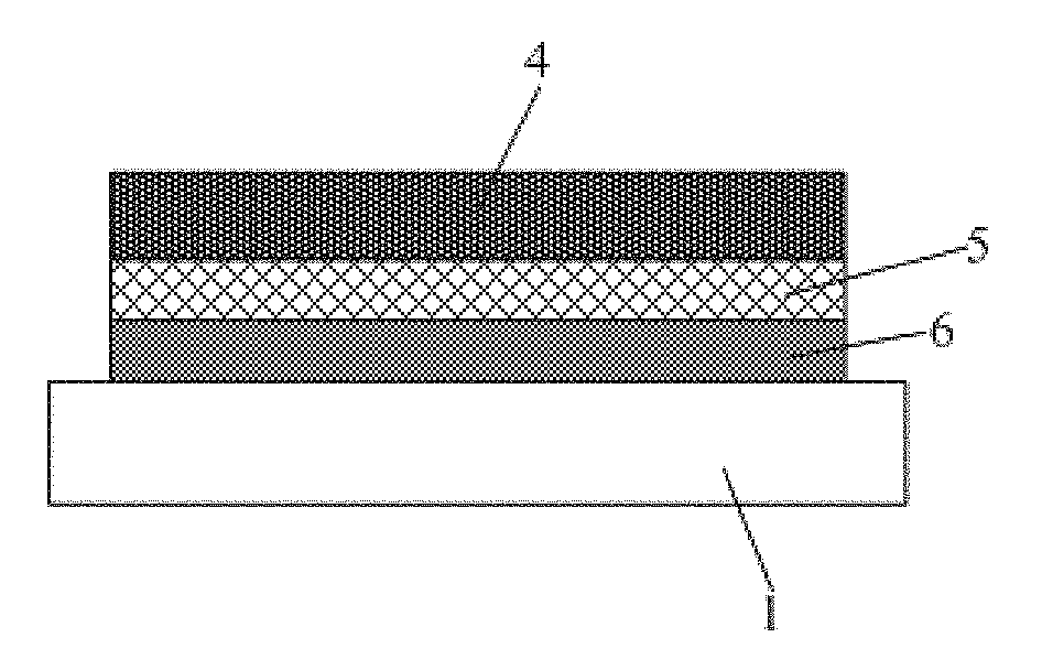
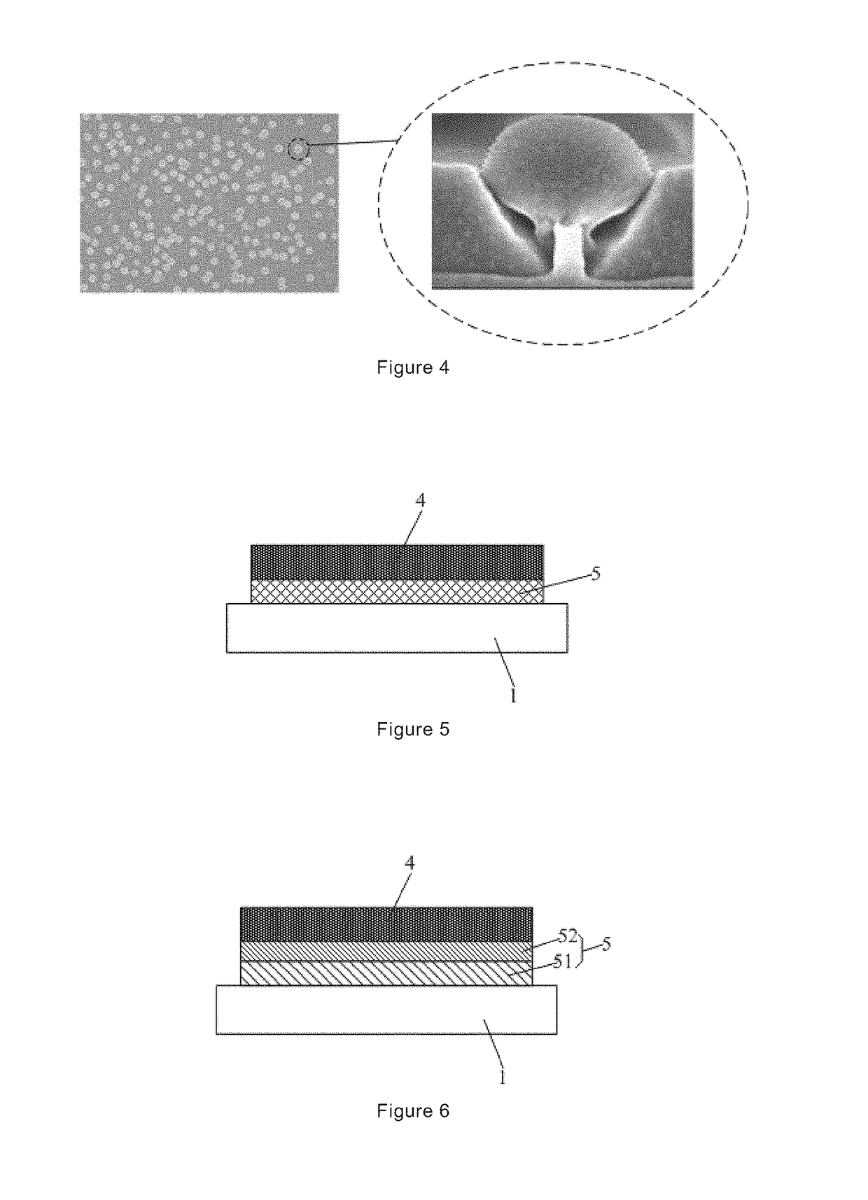
[0028]The present disclosure provides an array substrate and a method for manufacturing the same as well as a display device in order to solve the above technical problem present in the prior art. The array substrate comprises a substrate, a metal conductive film layer, and an anti-reflective film layer which is located between the substrate and the metal conductive film layer.
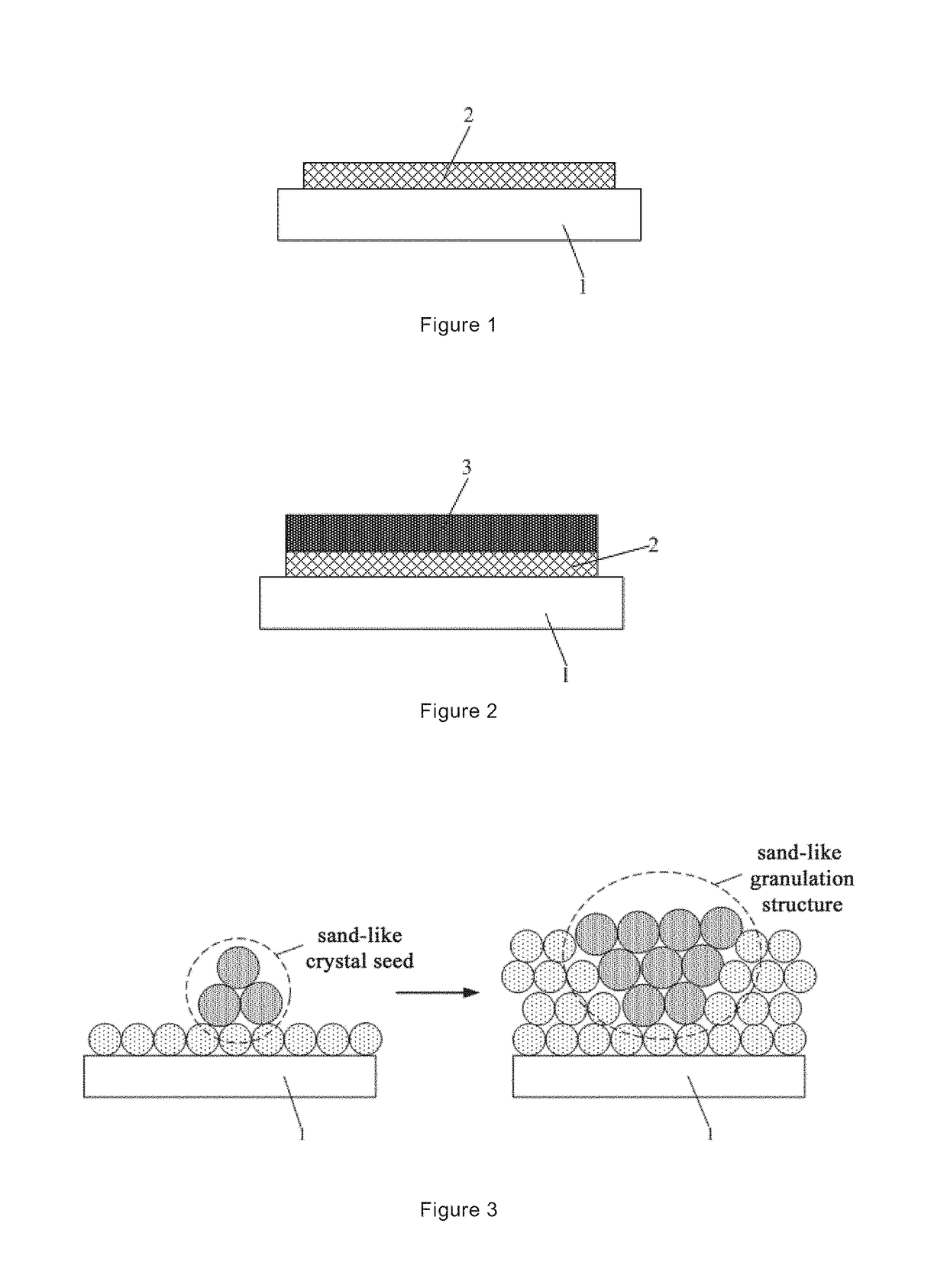
[0029]Herein, the term “sand-like granulation structure” refers to, an uneven structure like sand grain in the thin film formed by using a chemical vapor deposition process, which is produced due to the film formation abnormity caused by the sudden change of parameters such as electrical source power, gas flow and the like during the film formation.
[0030]The array substrate and the method for manufacturing the same, and the display device provided in the present disclosure will be described in detail with reference to the accompanying drawings and specific embodiments in order to provide a better understanding...
PUM
| Property | Measurement | Unit |
|---|---|---|
| Fraction | aaaaa | aaaaa |
| Fraction | aaaaa | aaaaa |
| Time | aaaaa | aaaaa |
Abstract
Description
Claims
Application Information