
Pellicle frame and pellicle

a pellicle and frame technology, applied in the field of pellicle for lithography, can solve the problems of poor processing efficiency, poor quality, or the like, and the edge of the pattern becomes rough, and achieves excellent processability, wrinkles or breakage, and suppressed distortion of the pellicle frame

Active Publication Date: 2019-04-11
SHIN ETSU CHEM IND CO LTD
View PDF0 Cites 1 Cited by
  • Summary
  • Abstract
  • Description
  • Claims
  • Application Information

AI Technical Summary

Benefits of technology

[0029]According to the pellicle frame and pellicle of the present invention, even if the temperature of a pellicle frame is increased by the light energy due to exposure, expansion and contraction, and distortion of the pellicle frame can be suppressed to be lower, and wrinkles or breakage is not generated in a pellicle film. In addition, since the pellicle frame and pellicle accordi

Problems solved by technology

When a semiconductor device such as LSI and VLSI, a liquid crystal display, or the like is produced, a pattern is formed by irradiating a semiconductor wafer or an original plate for liquid crystal with light, and if dust adheres to a photomask or a reticle (hereinafter, simply referred to as a “photomask”), which is to be used at this time, the edge of the pattern becomes rough, and further there is a problem that the dimension, the quality, the appearance, or the like is impaired, for example, the base becomes black and dirty.
For this reason, the pattern formation work is usually performed in a clean room, however, it is still difficult to keep the photomask clean.
However, for a next-generation semiconductor device or liquid crystal display, further miniaturized pattern formation of 10 nm or less is required, and it is no longer possible to form such a miniaturized pattern of 10 nm or less by the improvement of a conventional exposure technique using an excimer laser.
With respect to a pellicle that affect the yield of a semiconductor device or a liquid crystal display, for example, in Patent Document 3, a silicon film having a thickness of 0.1 to 2.0 μm that is transparent and does not cause optical distortion is described as a pellicle film to be used for EUV lithography, however, in order to apply in practice, unresolved problems still remain and are a major obstacle to put

Method used


Image

  • Pellicle frame and pellicle
  • Pellicle frame and pellicle

Examples


example 1

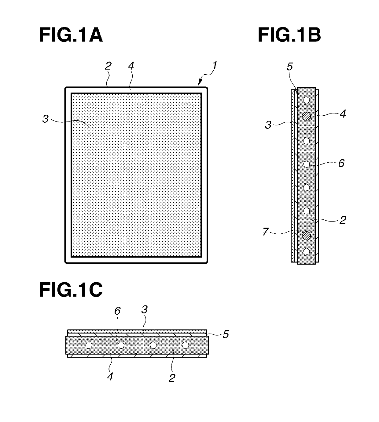
[0058]A pellicle frame (with an outer size of 150 mm×118 mm×1.5 mm, and a frame width of 3.0 mm) made of titanium (having a linear expansion coefficient of 8.4×10⁻⁶ (1 / K), and a density of 4.5 g / cm3) was prepared.

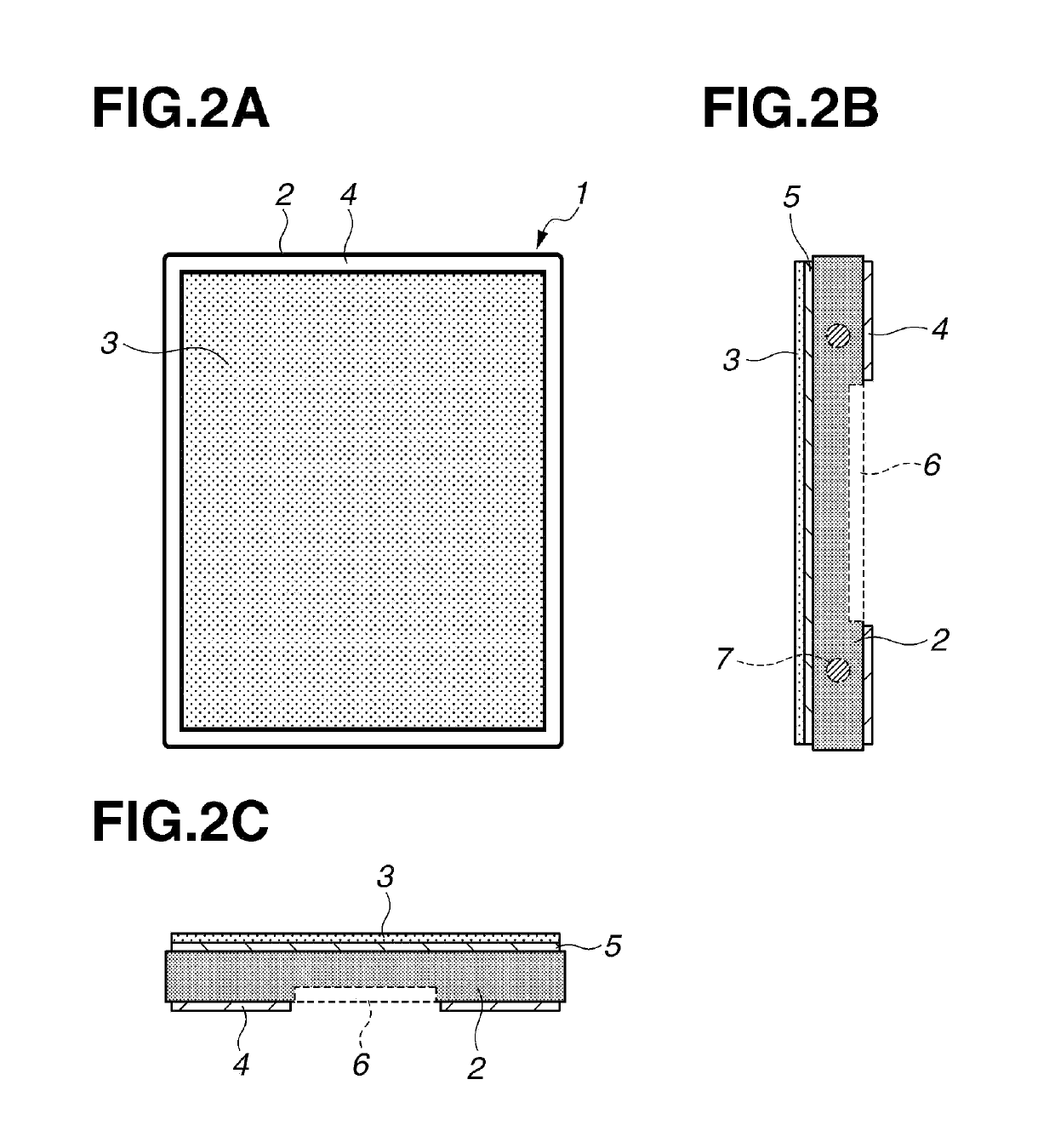
[0059]On an outer side face of the long side of the pellicle frame, two jig holes each having a diameter of 1 mm and a depth of 1.2 mm were provided at two places each with a distance of 52 mm away from the center of the side in the corner direction. In addition, six through holes were provided at six places with a distance of 10 mm, 30 mm, and 65 mm, respectively away from the center of the long side in the corner direction, and four through holes were provided at four places with a distance of 10 mm, and 30 mm, respectively away from the center of the short side in the corner direction.

[0060]This pellicle frame was washed with a neutral detergent and pure water, and dried, and then a silicone pressure-sensitive adhesive (X-40-3264 manufactured by Shin-Etsu Chemical Co., L...

example 2

[0063]As the material for a pellicle frame, a Ti—Al6-V4 titanium alloy (having a linear expansion coefficient of 8.8×10⁻⁶ (1 / K), and a density of 4.4 g / cm3), which is an alloy of titanium, aluminum and vanadium, was used. Except for the above-described material for a pellicle frame, a pellicle was prepared in a similar manner as in Example 1.


PUM


Abstract

The present invention is to provide a pellicle frame characterized by including a metal or alloy having a linear expansion coefficient of 10×10′ (1/K) or less and further a density of 4.6 g/cm3 or less, and a pellicle characterized by including the pellicle frame as an element.

Description

CROSS-REFERENCE TO RELATED APPLICATION[0001]This non-provisional application claims priority under 35 U.S.C. § 119(a) on Patent Application No. 2017-197004 filed in Japan on Oct. 10, 2017, the entire contents of which are hereby incorporated by reference.TECHNICAL FIELD[0002]The present invention relates to a pellicle for lithography used as a dust guard when a semiconductor device such as large scale integration (LSI) and very large scale integration (VLSI), a printed board, a liquid crystal display, or the like is produced.BACKGROUND ART[0003]When a semiconductor device such as LSI and VLSI, a liquid crystal display, or the like is produced, a pattern is formed by irradiating a semiconductor wafer or an original plate for liquid crystal with light, and if dust adheres to a photomask or a reticle (hereinafter, simply referred to as a “photomask”), which is to be used at this time, the edge of the pattern becomes rough, and further there is a problem that the dimension, the quality,...

Claims


Application Information

Patent Timeline
IPC IPC(8): G03F1/64
CPCG03F1/64G03F1/62G03F7/70983
Inventor YANASE, YU
Owner SHIN ETSU CHEM IND CO LTD
Learn More