Nano-compound field-effect transistor and manufacturing method therefor

a field-effect transistor and nano-compound technology, applied in the field of field-effect transistors, can solve the problems of difficult uniform channel formation, low stability of channel formed with carbon nanotubes (cnt) according to the related art, and reach the limit of field-effect transistor miniaturization, etc., to achieve convenient and economic manufacture, the effect of reducing the cost of manufacturing

Inactive Publication Date: 2019-04-18
NDD
View PDF3 Cites 2 Cited by
  • Summary
  • Abstract
  • Description
  • Claims
  • Application Information

AI Technical Summary

Benefits of technology

[0012]According to the present invention, a nano-compound field-effect transistor may be manufactured conveniently and economically, and therefore, measuring devices using the nano-compound field-effect transistor may be manufactured inexpensively and conveniently.

Problems solved by technology

Miniaturization of field-effect transistors is reaching more and more limitations.
However, according to the related art, it is difficult for the carbon nanotube (CNT) to be uniformly applied onto an insulating film, and therefore, it is difficult to uniformly form a channel.
Therefore, the stability of the channel formed with the carbon nanotube (CNT) according to the related art is very low, and it is thus difficult to commercialize the biosensor that uses the CNT-FET.

Method used


Image

  • Nano-compound field-effect transistor and manufacturing method therefor
  • Nano-compound field-effect transistor and manufacturing method therefor
  • Nano-compound field-effect transistor and manufacturing method therefor

Examples


Embodiment Construction

[0017]Hereinafter, embodiments of the present invention will be described in detail with reference to the accompanying drawings.

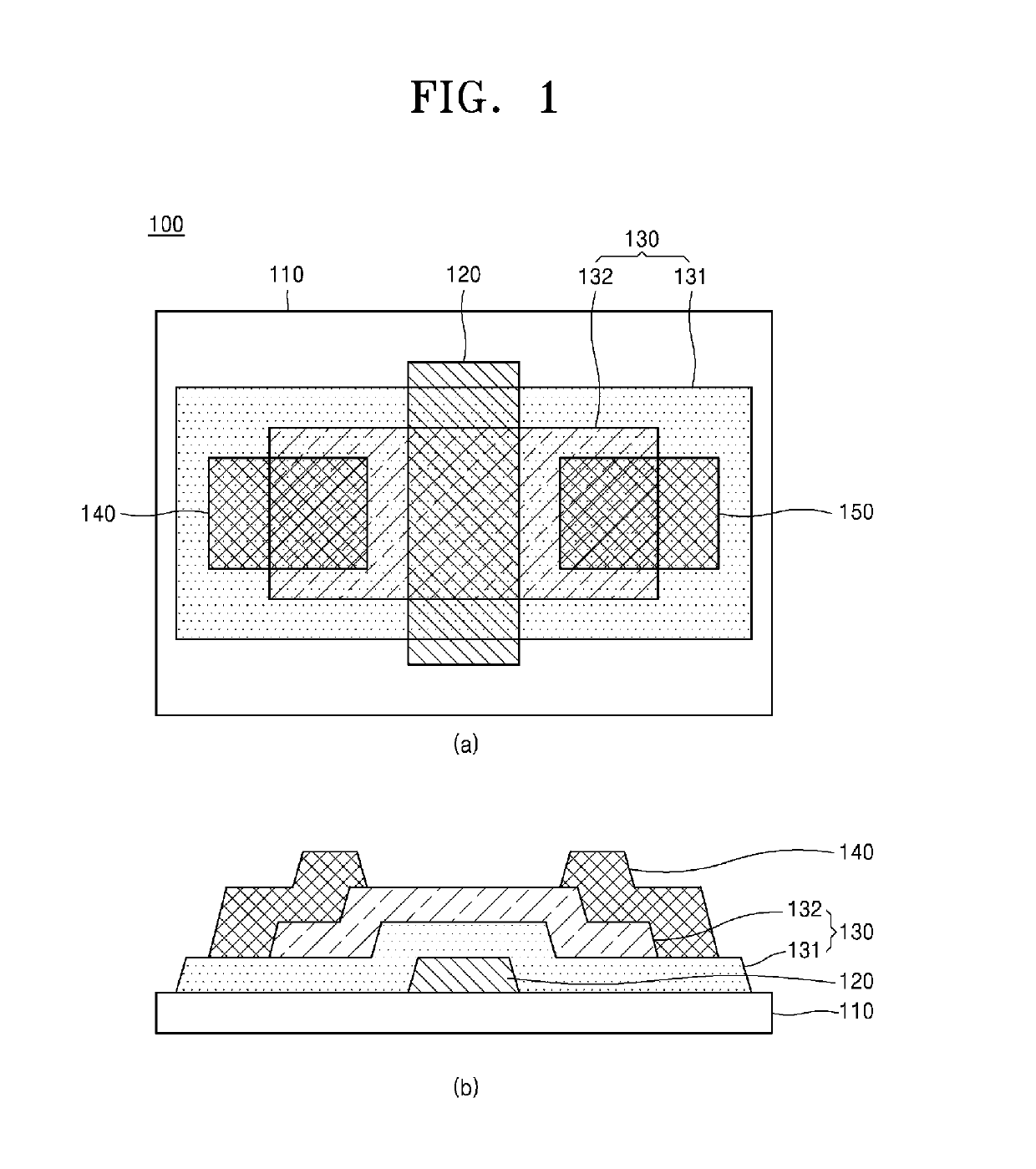
[0018]FIG. 1 is an exemplary view illustrating the configuration of a nano-compound field-effect transistor according to the present invention. (a) of FIG. 1 is a plane view of the nano-compound field-effect transistor according to the present invention, and (b) of FIG. 1 is a cross-sectional view of the nano-compound field-effect transistor according to the present invention.

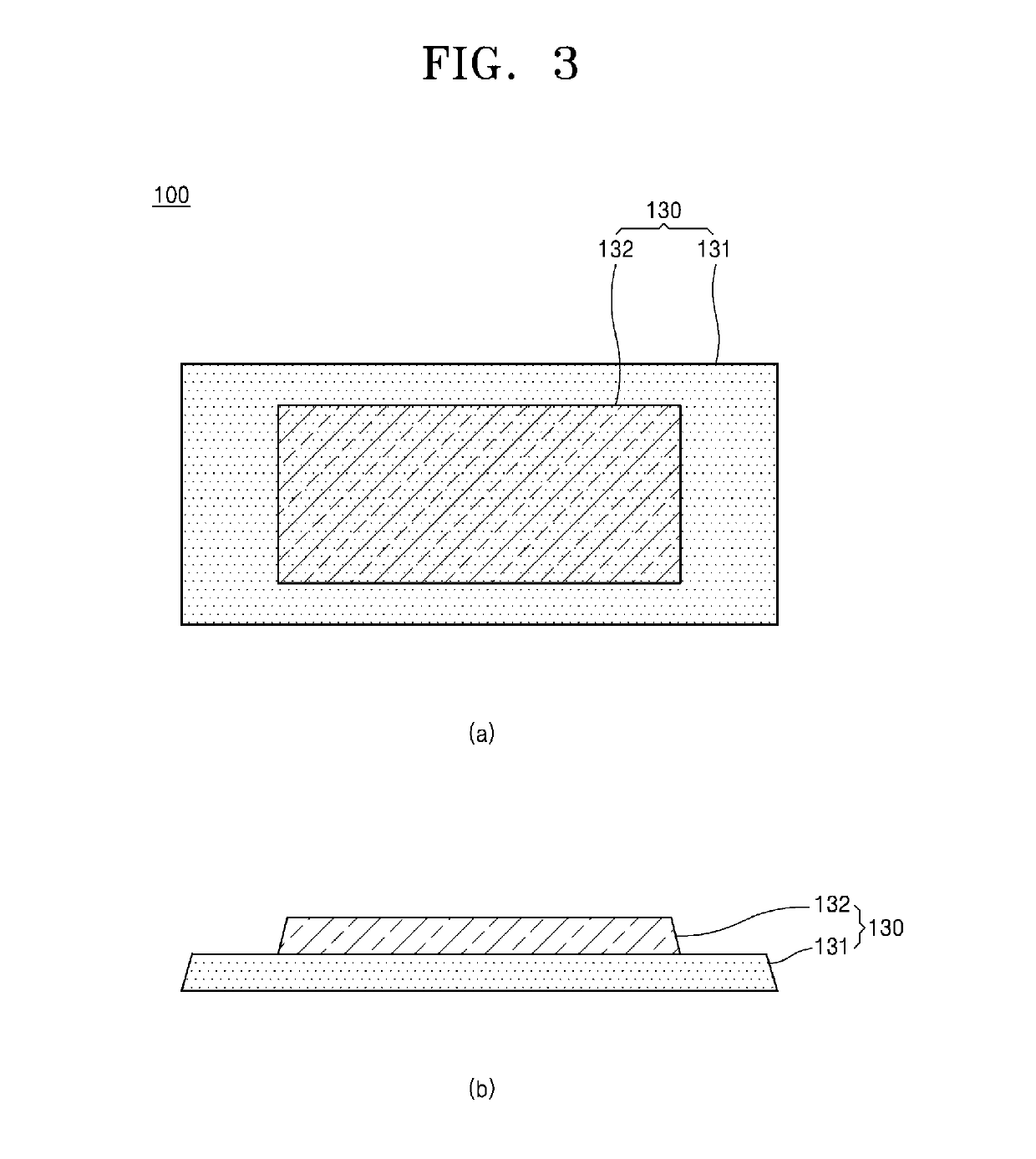
[0019]According to the present invention, a nano-compound field-effect transistor 100, as illustrated in (a) and (b) of FIG. 1, includes a gate 120 on a substrate 110, a channel part 130 bonded on the gate so as to overlap with the gate 120, a source 140 at one end of the channel part 130, and a drain facing the source at the other end of the channel part with the gate disposed therebetween.

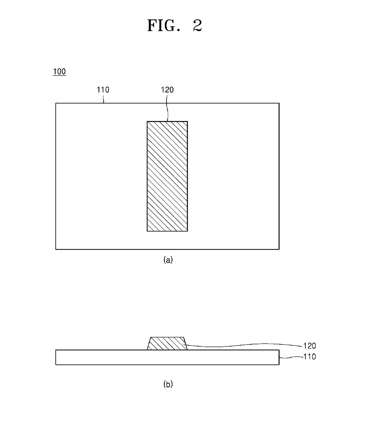
[0020]First, the substrate 110 may be any one among a Si wafer, glass, a PDMS, a PMMA, a PCB, an...


PUM

PropertyMeasurementUnit
flexibleaaaaaaaaaa
stabilityaaaaaaaaaa
insulatingaaaaaaaaaa

Abstract

The purpose of the present invention is to provide a nano-compound field-effect transistor formed by fusing, on a gate, a channel part having a nano-compound coated on an insulating film, and a manufacturing method therefor. To this end, a nanocompound field-effect transistor, according to the present invention, has: a gate formed on a substrate; a channel part bonded on the gate so as to be overlapped on the gate; a source formed on one end of the channel part; and a drain formed so as to face the source at the other end of the channel part by having the gate interposed therebetween, wherein the channel part comprises an insulating film and a nano-compound coated on the insulating film, the insulating film is bonded to the gate and the substrate, and the source and the drain are overlapped on the nano-compound.

Description

TECHNICAL FIELD[0001]The present invention relates to a field-effect transistor and a manufacturing method therefor, and more particularly, to a nano-compound field-effect transistor which can be used as a sensor and a manufacturing method therefor.[0002]This application claims priority based on the Korea Patent Application No. 10-2016-0158904, filed on Nov. 28, 2016, the entire contents of which are incorporated herein by reference.BACKGROUND ART[0003]Miniaturization of field-effect transistors is reaching more and more limitations.[0004]As a way to overcome the limitations on the miniaturization of the field-effect transistors, a carbon nanotube (CNT), graphene, MoS2, or the like has been proposed, and an integrated circuit (IC) using the same has also been developed.[0005]In particular, since a semiconductor chip including the field-effect transistor using the carbon nanotube (hereinafter, simply referred to as a CNT-FET) may be used as a biosensor, studying on the CNT-FET is bei...

Claims


Application Information

Patent Timeline
Patent Type & Authority Applications(United States)
IPC IPC(8): H01L21/268H01L29/10H01L29/772B23K26/00
CPCH01L21/268H01L29/10H01L29/772B23K26/0006H01L29/66969H01L29/778H01L29/78681H01L29/78696H01L29/4908H01L29/66742H01L29/1606H01L29/24H01L29/66045H10K85/221H10K10/471H10K10/484H01L29/0665H01L29/1025H01L29/786
Inventor AHN, SAE YOUNGKWON, HYUN HWA
Owner NDD
Why Eureka
Try Eureka