

Low gate current junction field effect transistor device architecture
a transistor and junction field technology, applied in the direction of semiconductor devices, basic electric elements, electrical equipment, etc., can solve the problem of depletion of the top ga
- Summary
- Abstract
- Description
- Claims
- Application Information
AI Technical Summary
Benefits of technology
Problems solved by technology
Method used
Image

Examples
Embodiment Construction
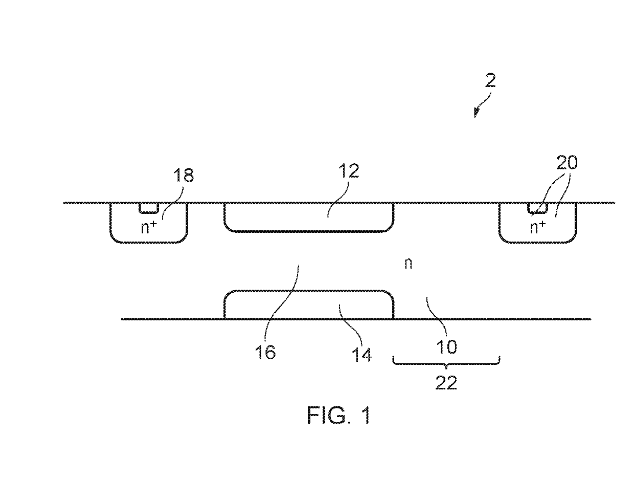
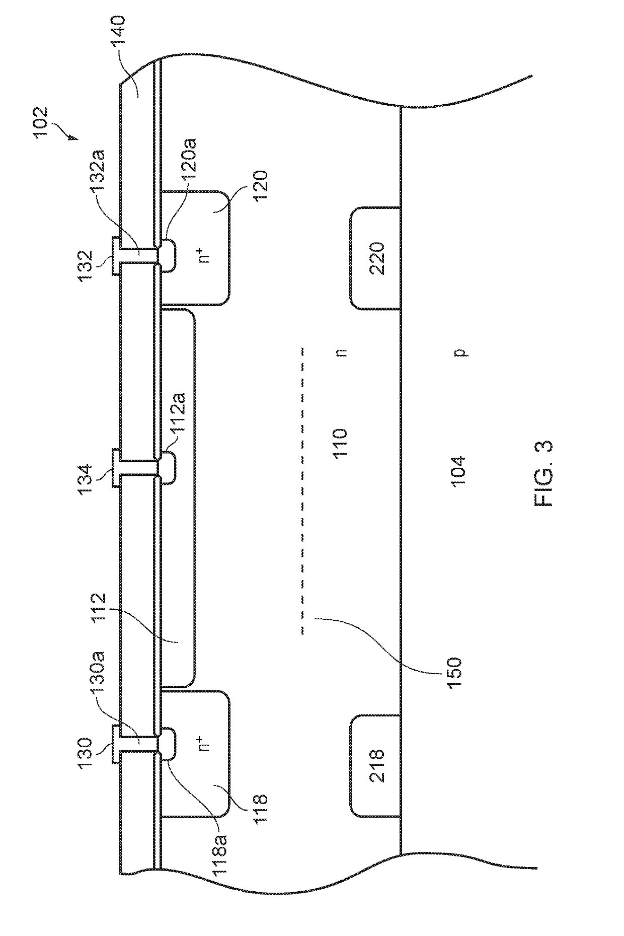
[0023]In the Figures some of the device structures, such as regions of doped material are delimited by lines. These boundaries are representative only and it should be appreciated that the doping concentration may vary over a distance giving rise to a blurring of the transition between P type and N type regions rather that giving rise to a distinct boundary.
[0024]Terms such as “above”, “below”, “to the right hand side of” and the like refer to the relative placement of features in the drawings when the drawings are in an upright orientation. Such terms are not limiting of the positions of components or regions within a device in accordance with the teachings of this disclosure unless the device has been orientated so as to match the orientation of an equivalent one of the drawings.
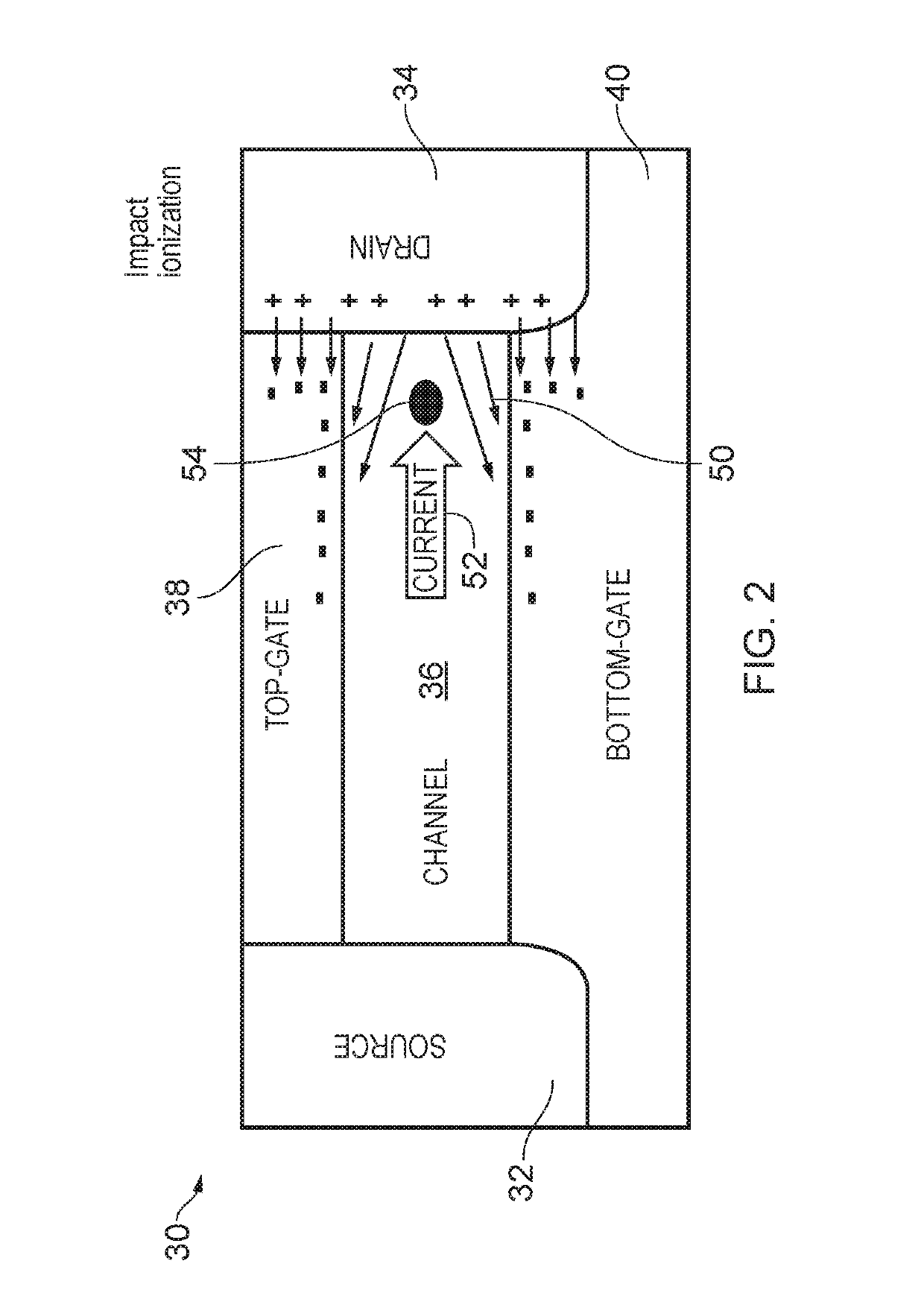
[0025]Despite the apparent disadvantages of the JFET in terms of its ability to draw an additional gate current compared to a MOSFET as set out above, it still remains in use because the JFET can offer bet...
PUM
 Abstract
Description
Claims
Application Information