Unlock instant, AI-driven research and patent intelligence for your innovation.

Pixel array substrate and display device

a technology of pixel array substrate and display device, which is applied in the direction of semiconductor devices, instruments, electrical devices, etc., can solve the problems of fluctuation disturbance of signals, affecting display quality, and increasing the demand for display panel of display device without frames on margins, so as to reduce coupling induction

Active Publication Date: 2019-05-09
E INK HLDG INC
View PDF0 Cites 0 Cited by
  • Summary
  • Abstract
  • Description
  • Claims
  • Application Information

AI Technical Summary

Benefits of technology

The patent provides a pixel array substrate that reduces interference between scan lines, resulting in better display quality. The distance between adjacent scan lines is set to be between one-third and one-half of the distance between adjacent pixel structures. This prevents signal distortion caused by interference between scan lines and improves the performance of display devices that use this substrate.

Problems solved by technology

With the development of display technology and diversification of various display devices, in order to obtain a larger image display area in a display device having limited volume, demand for the display panel of the display device without frames on margins grows more and more desperate.
However, for the layout of a circuit meeting the demand for the frameless display panel, coupling induction between adjacent lines transmitting different drive signals often causes a fluctuation disturbance in signals, so display quality is affected.

Method used


Image

  • Pixel array substrate and display device
  • Pixel array substrate and display device
  • Pixel array substrate and display device

Examples


Embodiment Construction

[0026]Reference will now be made in detail to the present preferred embodiments of the disclosure, examples of which are illustrated in the accompanying drawings.

[0027]Wherever possible, the same reference numbers are used in the drawings and the description to refer to the same or like parts.

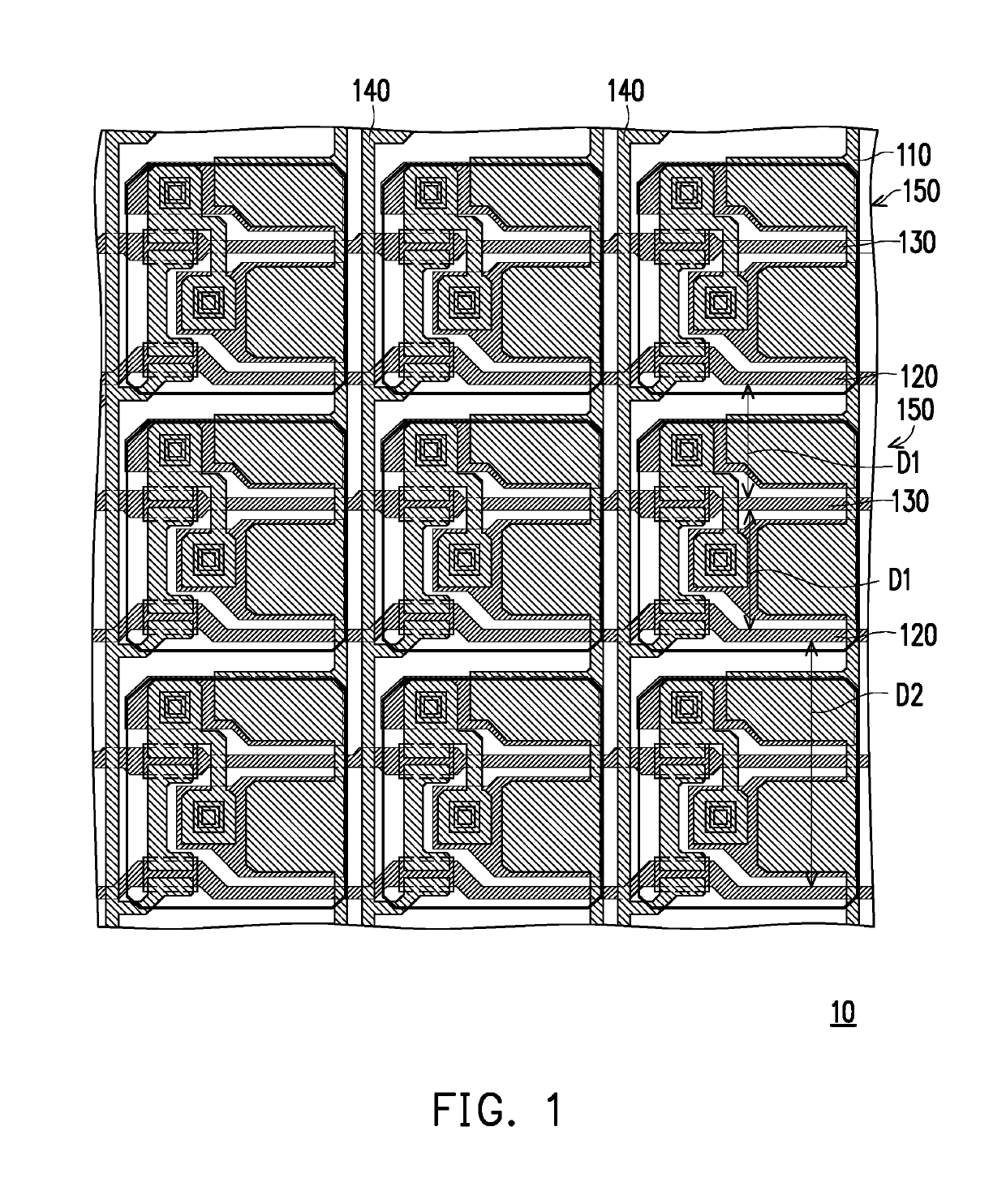
[0028]FIG. 1 is a top view of a display device according to an embodiment of the disclosure. FIG. 2 is a partially enlarged view of the display device of FIG. 1. FIG. 3 is a cross-sectional view taken along line A-A′ of the display device of FIG. 2. FIG. 4 is a cross-sectional view taken along line B-B′ of the display device of FIG. 2. FIGS. 3 and 4 are drawings showing the cross section of the display device taken along the lines A-A′ and B-B′ respectively. For illustration purpose, some elements are omitted from FIGS. 1 and 2 (such as a display medium 200 shown in FIGS. 3 and 4). The display device 10 according to the embodiment of the disclosure includes a pixel array substrate 100 and the d...


PUM


Abstract

A pixel array substrate includes a substrate, first and second scan lines, data lines, and pixel structures. The first and second scan lines are disposed alternately and are enabled for different time durations in the same frame time. The data lines intersect with the first and second scan lines. Each of the pixel structures includes first and second active devices, and a pixel electrode. The first and second active devices are turned on and off by the first and second scan lines, respectively. The pixel electrode is connected to the first active device which is connected to one of the data lines by being connected to the second active device. A distance between the first and second scan lines adjacent to each other is a third to a half of a pitch of the pixel structures.

Description

CROSS-REFERENCE TO RELATED APPLICATION[0001]This application claims the priority benefit of China application serial no. 201711088519.X, filed on Nov. 8, 2017. The entirety of the above-mentioned patent application is hereby incorporated by reference herein and made a part of this specification.BACKGROUND OF THE DISCLOSURE1. Field of the Disclosure[0002]The disclosure relates to a pixel array substrate and a display device.2. Description of Related Art[0003]With the development of display technology and diversification of various display devices, in order to obtain a larger image display area in a display device having limited volume, demand for the display panel of the display device without frames on margins grows more and more desperate. However, for the layout of a circuit meeting the demand for the frameless display panel, coupling induction between adjacent lines transmitting different drive signals often causes a fluctuation disturbance in signals, so display quality is affec...

Claims


Application Information

Patent Timeline
Patent Type & Authority Applications(United States)
IPC IPC(8): G09G3/20H01L27/12
CPCG09G3/20H01L27/124G09G2300/0439G09G2300/0426G09G2310/0278G09G2300/0809G09G2310/0218G09G2330/06
Inventor TSAI, SHU-FENCHEN, JIA-HUNGLIANG, KUANG-HENGWANG, CHIH-CHINGFRENCH, IAN
Owner E INK HLDG INC
Features
  • R&D
  • Intellectual Property
  • Life Sciences
  • Materials
  • Tech Scout
  • Unparalleled Data Quality
  • Higher Quality Content
  • 60% Fewer Hallucinations
Learn More