
Solid state storage device and program loading method thereof

Active Publication Date: 2019-05-23
SOLID STATE STORAGE TECH CORP
View PDF3 Cites 0 Cited by
  • Summary
  • Abstract
  • Description
  • Claims
  • Application Information

AI Technical Summary

Benefits of technology

The present invention provides a solid state storage device and a program loading method. The device does not have a read-only memory and the specified program is stored in a non-volatile memory. The binary code of the program is stored in a specific way to make the device cost-effective. The program can be successfully loaded into the control circuit and the device can operate normally.

Problems solved by technology

The solid state storage device is not equipped with a read only memory.

Method used


Image

  • Solid state storage device and program loading method thereof
  • Solid state storage device and program loading method thereof
  • Solid state storage device and program loading method thereof

Examples


first embodiment

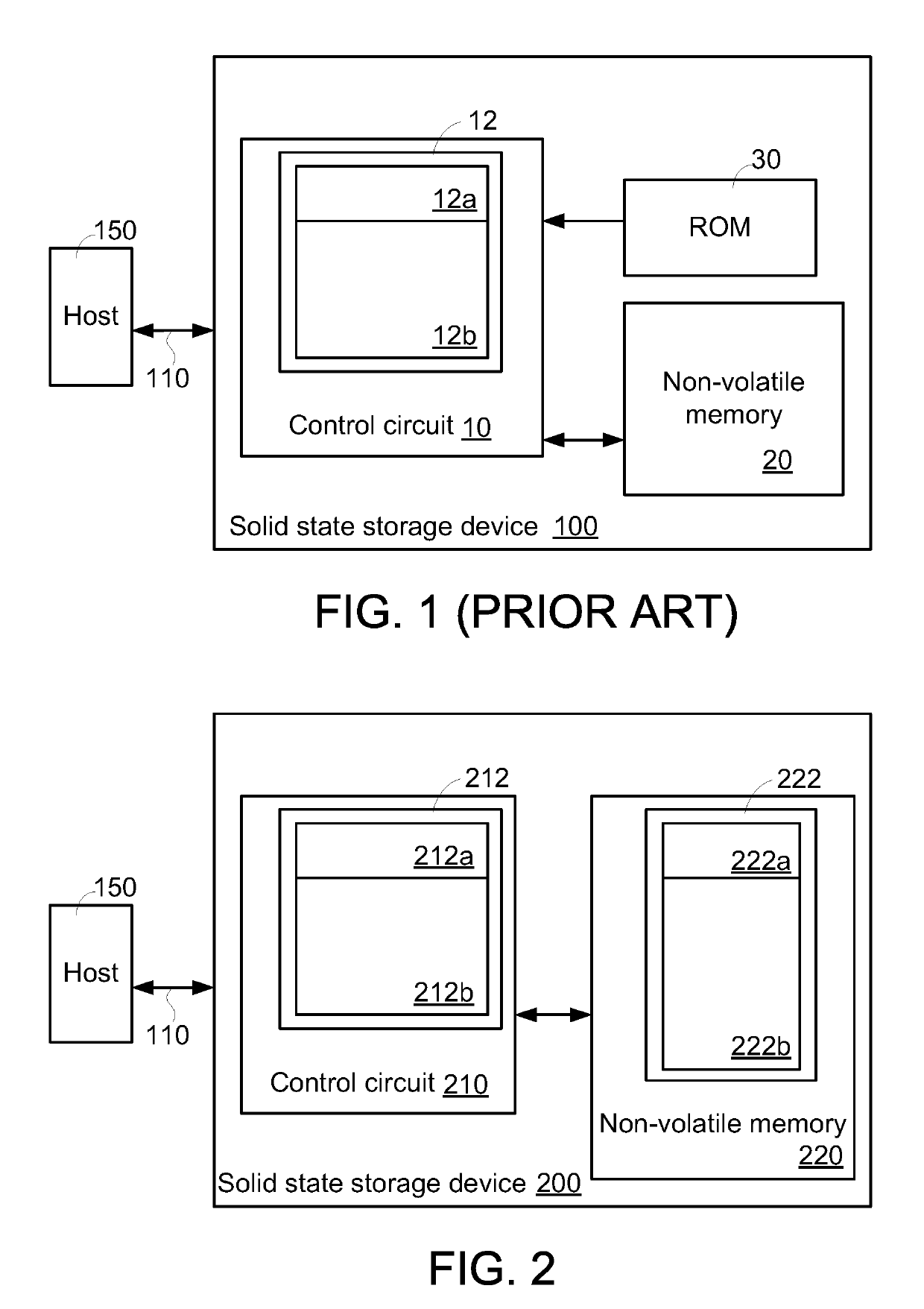
[0025]FIG. 2 is a schematic functional block diagram illustrating the architecture of a solid state storage device according to the present invention. As shown in FIG. 2, the solid state storage device 200 comprises a control circuit 210 and a non-volatile memory 220. The non-volatile memory 220 is connected with the control circuit 210. Moreover, the non-volatile memory 220 further comprises a memory cell array 222.

[0026]The solid state storage device 200 is connected with a host 150 through an external bus 110. For example, the external bus 110 is a USB bus, an SATA bus, a PCIe bus, an M.2 bus, a U.2 bus, or the like.

[0027]The control circuit 210 comprises a storage unit 212. The storage unit 212 comprises a first storage zone 212a and a second storage zone 212b. After the control circuit 210 is produced, a boot code loader has been stored in the first storage zone 212a in order to enable the solid state storage device 200. Generally, the first storage zone 212a is set as a read-o...

second embodiment

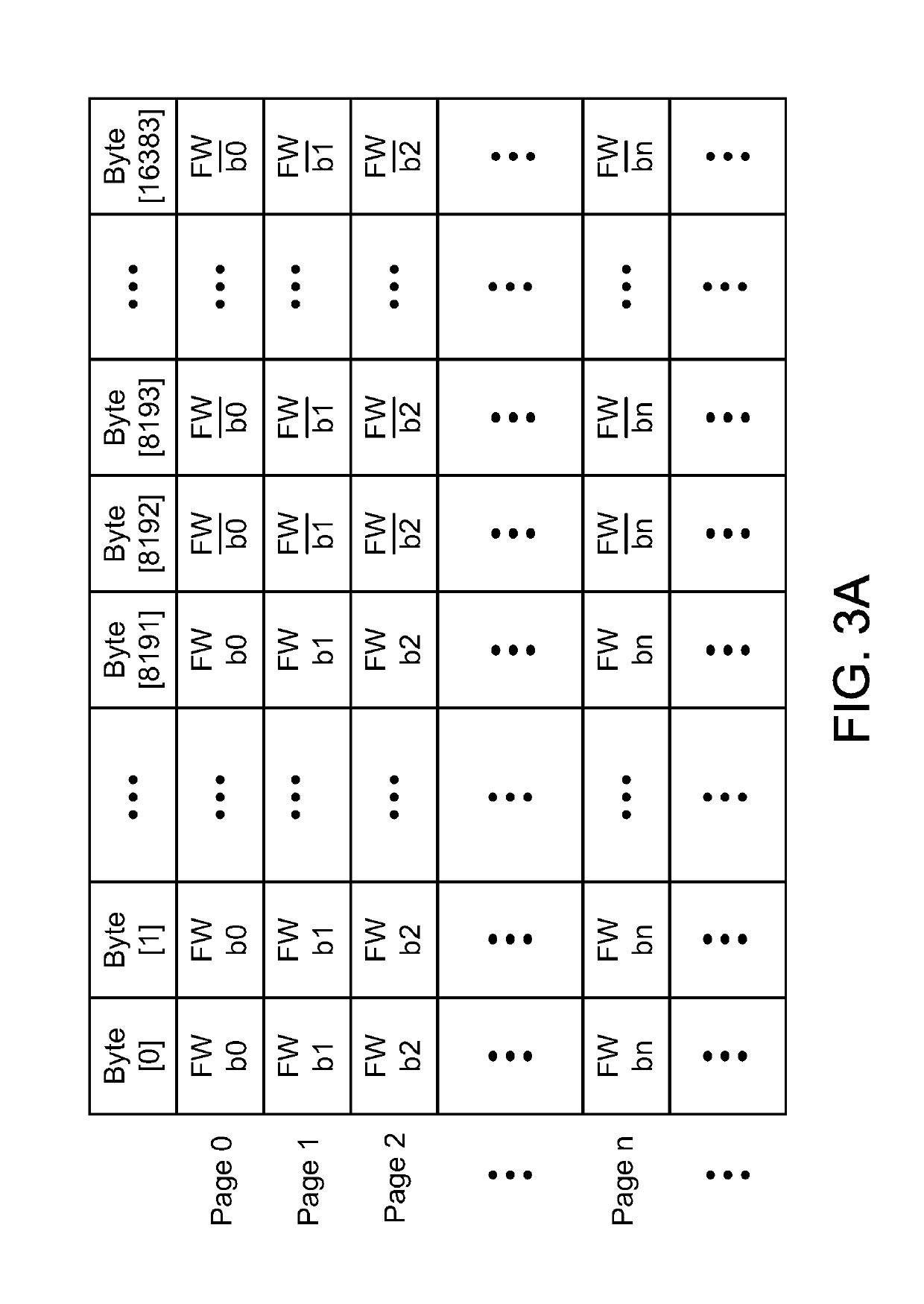
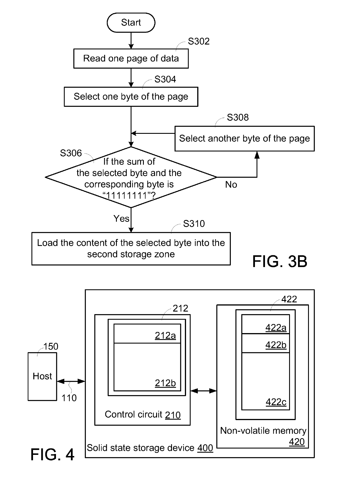
[0064]FIG. 5A schematically illustrates the data structure of the configuration program stored in the third storage zone of the memory cell array of the solid state storage device according to the present invention. The memory cell array 422 contains 1024 blocks, and each block contains 256 pages. Each page is typically 16 k bytes in size.

[0065]In an embodiment, one-byte binary code of the configuration program is repeatedly stored in the one-page space of the third storage zone 422a. That is, one-page space of the third storage zone 422a stores one-byte binary code of the configuration program. For example, the size of the configuration program is 265 bytes. That is, the configuration program is composed of 265 binary codes. Consequently, the third storage zone 4222a needs 256 pages of space to store the configuration program. The capacity of the third storage zone 422a is 4 Mbytes (i.e., 256×16 kbyte=4 Mbytes). That is, the configuration program with a size of 256 bytes is stored ...


PUM


Abstract

A solid state storage device includes a control circuit and a non-volatile memory. The control circuit includes a first storage zone and a second storage zone. A boot code loader is stored in the first storage zone. The non-volatile memory includes a memory cell array. The memory cell array includes a third storage zone and a fourth storage zone. A specified program is stored in the third storage zone. The third storage zone contains a first block. A first page of the first block is divided into a first portion and a second portion. A first binary code of the specified program is repeatedly stored in plural bytes of the first portion of the first page. The one's complement of the first binary code is repeatedly stored in plural bytes of the second portion of the first page.

Description

[0001]This application claims the benefit of People's Republic of China Patent Application No. 201711181808.4, filed Nov. 23, 2017, the subject matter of which is incorporated herein by reference.FIELD OF THE INVENTION[0002]The present invention relates to a solid state storage device and a control method, and more particularly to a solid state storage device and a program loading method.BACKGROUND OF THE INVENTION[0003]As is well known, solid state storage devices such as SD cards or solid state drives (SSD) are widely used in various electronic devices. Generally, a solid state storage device comprises a controlling circuit and a non-volatile memory.[0004]FIG. 1 is a schematic functional block diagram illustrating the architecture of a conventional solid state storage device. As shown in FIG. 1, the solid state storage device 100 comprises a control circuit 10, a read only memory (ROM) 30 and a non-volatile memory 20. The non-volatile memory 20 is used for storing write data. A fi...

Claims


Application Information

Patent Timeline
IPC IPC(8): G06F9/445G06F3/06
CPCG06F9/445G06F3/0679G06F3/065G06F3/0625G06F3/0634G06F3/0632G06F9/4401
Inventor CHEN, PING-JIECHANG, SHENG-YUWENG, CHIEN-CHIH
Owner SOLID STATE STORAGE TECH CORP
Learn More