Micro lighting device

a micro-lighting and lighting device technology, applied in the direction of semiconductor devices, electrical apparatus, transistors, etc., can solve the problems of poor emission efficiency and half wavelength performance, low emission efficiency of front-emission micro-devices, and narrow viewing angles

Active Publication Date: 2019-06-20
ACER INC
View PDF2 Cites 0 Cited by
  • Summary
  • Abstract
  • Description
  • Claims
  • Application Information

AI Technical Summary

Benefits of technology

[0006]The present invention provides a micro lighting device which includes a substrate, an isolation layer formed on the substrate, a side-emission micro device, and a switching device. The side-emission micro device includes a first electrode, a second electrode and an emission surface, wherein the side-emission micro device is disposed in a way so that the emission surface is perpendicular to a surface of the substrate. The switching device includes a first end, a second end coupled to the first electrode, and a control end.
[0007]The present invention also provides a micro lighting device which includes a substrate, an isolation layer formed on the substrate, a side-emission micro device, a switching device, and at least one peripheral structure. The side-emission micro device includes a first electrode, a second electrode and an emission surface, wherein the side-emission micro device is disposed in a way so that the emission surface is parallel to a surface of the substrate. The switching device includes a first end, a second end coupled to the first electrode, and a control end. The at least one peripheral structure is covered by a reflective layer and includes a plurality of surfaces each at a specific angle with respect to the emission surface for adjusting a path of a beam emitted by the side-emission micro device.
[0008]The present invention also provides a micro lighting device which includes a substrate, an isolation layer formed on the first substrate, a side-emission micro device, a switching device, a first dielectric layer, and a second dielectric layer. The side-emission micro device includes a first electrode, a second electrode and an emission surface, wherein the side-emission micro device is disposed in a way so that the emission surface is parallel to a surface of the substrate. The switching device includes a first end, a second end coupled to the first electrode, and a control end. The first dielectric layer has a first refractive index. The second dielectric layer has a second refractive index different from the first refractive index so that a total reflection critical condition is satisfied when a beam emitted by the side-emission micro device arrives at the second dielectric layer after passing the first dielectric layer.

Problems solved by technology

Front-emission micro devices provide wider viewing angles, but have poor performances in emission efficiency and half wavelength.
Side-emission micro devices excel in high emission efficiency and better half wavelength, but can only provide narrower viewing angles.
Traditional micro LEDs normally adopt front-emission micro devices with low emission efficiency.

Method used


Image

  • Micro lighting device
  • Micro lighting device
  • Micro lighting device

Examples


Embodiment Construction

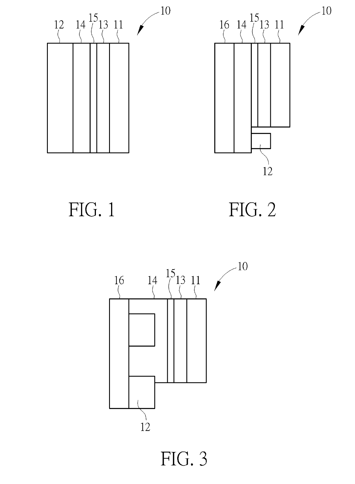
[0019]FIGS. 1˜3 are structural diagrams illustrating a side-emission micro device 10 according to embodiments of the present invention. In the present invention, the side-emission micro device 10 may be a micro LED device which is fabricated by combining P-type and N-type semiconductor materials before being mass transferred to a substrate (not shown).

[0020]In the embodiment illustrated in FIG. 1, the side-emission micro device 10 includes a first metal layer 11, a second metal layer 12, a first semiconductor layer 13, a second semiconductor layer 14, and a luminescent layer 15. The first metal layer 11 may serve as a P-electrode, and the second metal layer 12 may serve as an N-electrode. The first semiconductor layer 13 may include P-type dopants, and the second semiconductor layer 14 may include N-type dopants. The luminescent layer 15 maybe fabricated as an active layer with a multiple-quantum-well (MQW) structure whose wavelength is determined by the material band-gap. The lumin...


PUM


Abstract

A micro lighting device includes a substrate, an isolation layer formed on the substrate, a side-emission micro device, and a switching device. The side-emission micro device includes a first electrode, a second electrode and an emission surface. The side-emission micro device is disposed in a way so that the emission surface is perpendicular or parallel to the surface of the substrate. The switching device includes a first end, a second end coupled to the first electrode, and a control end.

Description

CROSS REFERENCE TO RELATED APPLICATION[0001]This application claims priority of Taiwan Application No. 106144546 filed on 2017, Dec. 19.BACKGROUND OF THE INVENTION1. Field of the Invention[0002]The present invention is related to a micro lighting device, and more particularly, to a micro lighting device which adopts side-emission micro devices.2. Description of the Prior Art[0003]Compared to traditional incandescent bulbs, light-emitting diodes (LEDs) are advantageous in low power consumption, long lifetime, small size, no warm-up time, fast reaction speed, and the ability to be manufactured as small or array devices. In addition to outdoor displays, traffic signs, and liquid crystal display (LCD) backlight for various electronic devices such as mobile phones, notebook computers or personal digital assistants (PDAs) , LEDs are also widely used as indoor / outdoor lighting devices in place of fluorescent of incandescent lamps. An LED may adopt front-emission micro devices or side-emiss...

Claims


Application Information

Patent Timeline
Patent Type & Authority Applications(United States)
IPC IPC(8): H01L33/60H01L29/06H01L27/15H01L33/36H01L33/62H01L33/06
CPCH01L33/60H01L29/0649H01L27/15H01L33/36H01L33/62H01L33/06H01L29/786H01L25/167
Inventor HSIANG, JUI-CHIEHCHEN, CHIH-CHIANG
Owner ACER INC
Why Eureka
Try Eureka