Display panel

a display panel and self-luminescent technology, applied in the field of display panels, can solve the problems of severe color shift of the amoled display panel, and achieve the effects of improving the viewing angle range, improving the color shift effect, and small cell gap

Active Publication Date: 2019-07-04
AU OPTRONICS CORP
View PDF10 Cites 10 Cited by
  • Summary
  • Abstract
  • Description
  • Claims
  • Application Information

AI Technical Summary

Benefits of technology

[0008]In view of the above, the display panel provided in an embodiment of the invention includes the active device located on the substrate, the first electrode electrically connected to the active device, the pixel definition layer having the first opening overlapped with the first electrode, the light emitting layer overlapped with the first opening and on the first electrode, the second electrode disposed on the light emitting layer, the shielding pattern layer disposed on the second electrode and having a second opening overlapped with the first opening, the first color filter pattern layer disposed on the second electrode and overlapped with the first opening and the second opening, and the second color filter pattern layer stacked with the first color filter pattern layer right above the shielding pattern layer. Hence, in comparison with the conventional display panel, the display panel described herein has a smaller cell gap and a better viewing angle range, such that the defect of color shift due to viewing angle change may be rectified.

Problems solved by technology

However, said BM may easily cause the AMOLED display panel severe color shift due to viewing angle change because the AMOLED display panel has a cell gap of up to about 18 μm.

Method used


Image

  • Display panel
  • Display panel
  • Display panel

Examples


Embodiment Construction

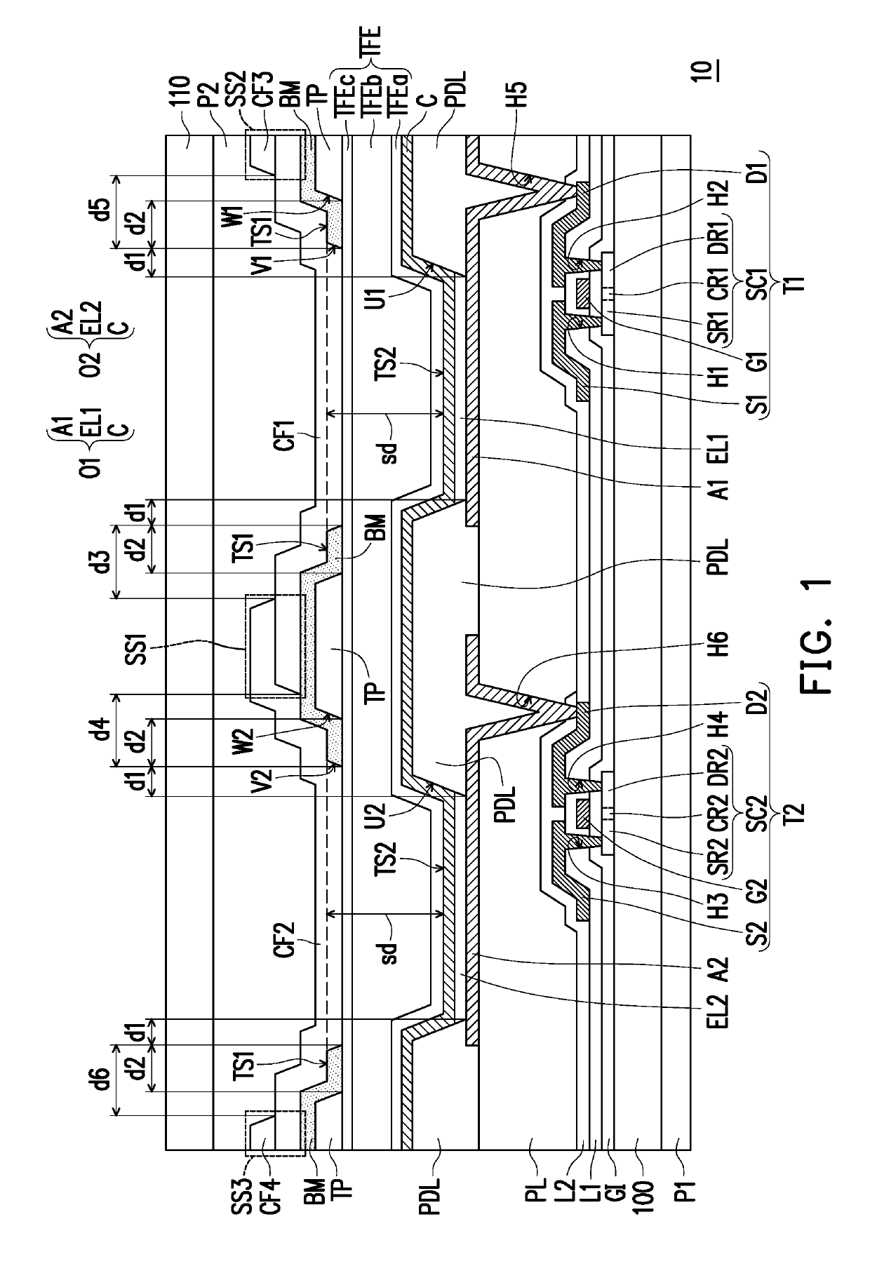
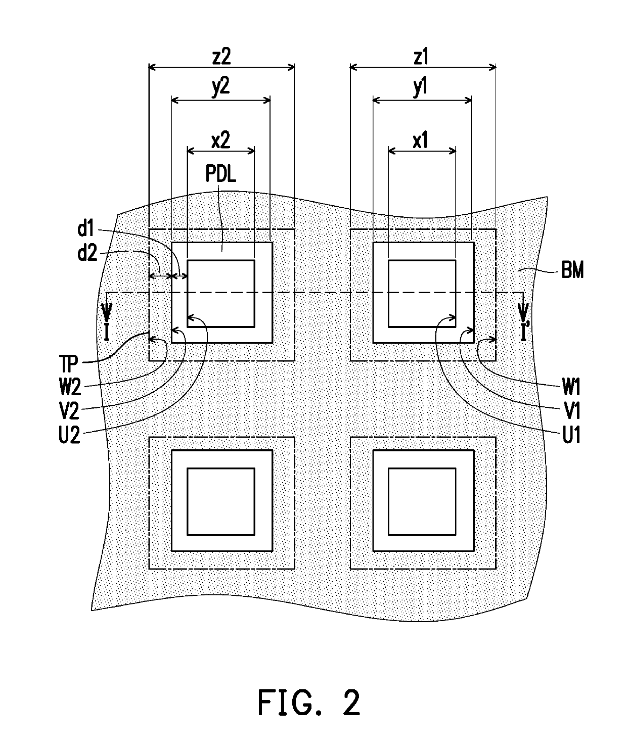
[0014]FIG. 1 is a schematic cross-sectional view of a portion of the display panel according to an embodiment of the disclosure. FIG. 2 is a schematic top view illustrating an arrangement of the pixel definition layer, the touch structure, and the shielding pattern layer depicted in FIG. 1. Note that the cross-sectional position shown in FIG. 1 may be referred to as the position of a sectional line I-I′ depicted in FIG. 2.

[0015]With reference to FIG. 1 and FIG. 2, the display panel 10 is a self-luminescent display panel, for instance. In the present embodiment, the display panel 10 is exemplified as an OLED display panel. The display panel 10 provided in the present embodiment includes a substrate 100, an active device T1, an active device T2, a first electrode A1, a first electrode A2, a pixel definition layer PDL, a light emitting layer EL1, a light emitting layer EL2, a second electrode C, a shielding pattern layer BM, a color filter pattern layer CF1, a color filter pattern laye...


PUM


Abstract

A display panel includes an active device disposed on a substrate, a first electrode electrically connected to the active device, a pixel definition layer, a light emitting layer, a second electrode, a shielding pattern layer, and first and second color filter pattern layers. The pixel definition layer has a first opening overlapped with the first electrode. At least a portion of the light emitting layer is disposed within the first opening and on the first electrode. The second electrode is disposed on the light emitting layer. The shielding pattern layer is disposed on the second electrode and has a second opening overlapped with the first opening. The first color filter pattern layer is disposed on the second electrode and overlapped with the first and second openings. The second color filter pattern layer is disposed on the second electrode. The first and second color filter pattern layers are stacked with each other right above the shielding pattern layer.

Description

CROSS-REFERENCE TO RELATED APPLICATION[0001]This application claims the priority benefit of Taiwan application serial no. 106146327, filed on Dec. 28, 2017. The entirety of the above-mentioned patent application is hereby incorporated by reference herein and made a part of this specification.TECHNICAL FIELD[0002]The disclosure relates to a display panel, and more particularly, to a self-luminescent display panel.RELATED ART[0003]In recent years, active matrix organic light-emitting diode (AMOLED) technologies continue to make breakthroughs, and the AMOLED has been successfully applied to portable display panels. At present, one of the commonly used technologies for making a full-color AMOLED display panel has applied a structure having a color filter layer and an organic light-emitting diode (OLED) which is used as a light source. To increase the contrast, said structure is often equipped with a black matrix (BM). However, said BM may easily cause the AMOLED display panel severe col...

Claims


Application Information

Patent Timeline
Patent Type & Authority Applications(United States)
IPC IPC(8): H01L27/32H01L51/52H01L27/146
CPCH01L27/323H01L51/5203H01L27/3246H01L27/14621H10K59/121H10K59/122H10K50/86H10K59/38H10K59/40H10K50/865H10K50/805
Inventor LIN, CHUN-YULEE, MENG-TING
Owner AU OPTRONICS CORP
Why Eureka
Try Eureka