Electronic component

a technology of electronic components and components, applied in the field of electronic components, can solve problems such as cracks in the element body, and achieve the effect of suppressing the occurrence of cracks

Active Publication Date: 2019-08-01
TDK CORPARATION
View PDF0 Cites 14 Cited by
  • Summary
  • Abstract
  • Description
  • Claims
  • Application Information

AI Technical Summary

Benefits of technology

[0003]An object of one aspect of the present invention is to provide an electronic component that suppresses occurrence of a crack in an element body.

Problems solved by technology

Therefore, a crack may occur in the element body with the end edge of the sintered metal layer as a starting point.

Method used


Image

  • Electronic component
  • Electronic component
  • Electronic component

Examples


first embodiment

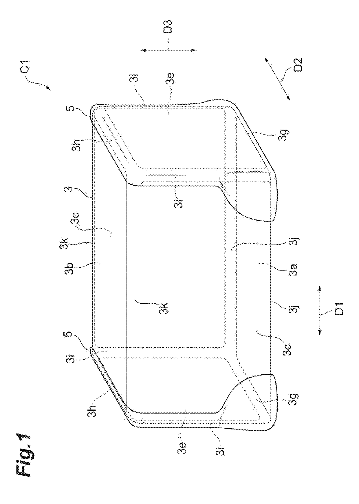
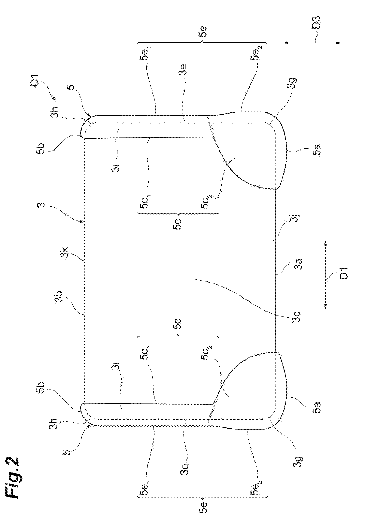
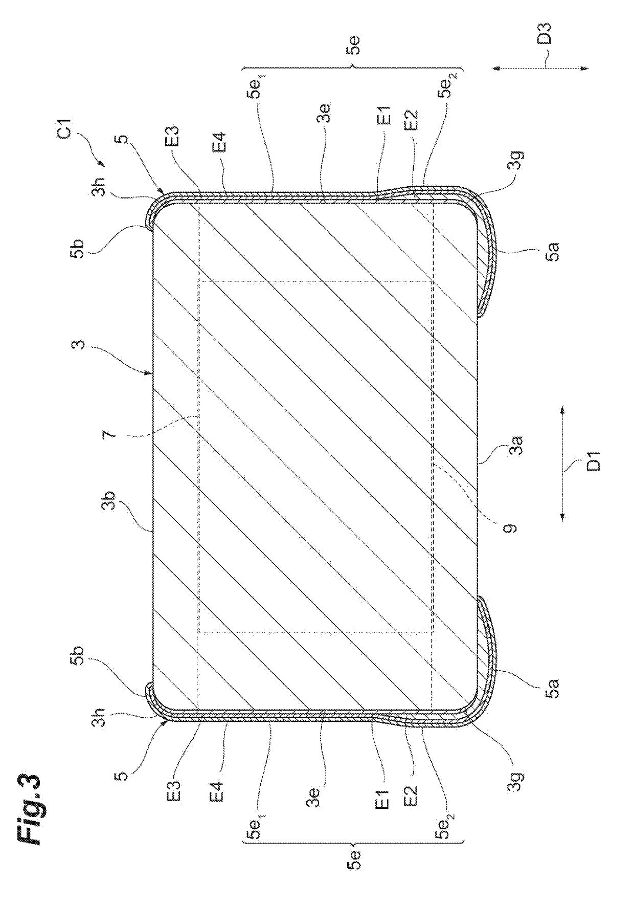
[0044]A configuration of a multilayer capacitor C1 according to a first embodiment will be described with reference to FIGS. 1 to 9. FIG. 1 is a perspective view of the multilayer capacitor according to the first embodiment. FIG. 2 is a side view of the multilayer capacitor according to the first embodiment. FIGS. 3 to 6 are views illustrating a cross-sectional configuration of the multilayer capacitor according to the first embodiment. FIG. 7 is a plan view illustrating an element body, a first electrode layer, and a second electrode layer. FIG. 8 is a side view illustrating the element body, the first electrode layer, and the second electrode layer. FIG. 9 is an end view illustrating the element body, the first electrode layer, and the second electrode layer. In the first embodiment, an electronic component is, for example, the multilayer capacitor C1.

[0045]As illustrated in FIG. 1, the multilayer capacitor C1 includes an element body 3 of a rectangular parallelepiped shape and a ...

second embodiment

[0105]A configuration of a multilayer capacitor C2 according to a second embodiment will be described with reference to FIGS. 11 to 22. FIG. 11 is a perspective view of the multilayer capacitor according to the second embodiment. FIG. 12 is a side view of the multilayer capacitor according to the second embodiment. FIGS. 13 to 18 are views illustrating a cross-sectional configuration of the multilayer capacitor according to the second embodiment. FIGS. 19 and 20 are plan views illustrating an element body, a first electrode layer, and a second electrode layer. FIG. 21 is a side view illustrating the element body, the first electrode layer, and the second electrode layer. FIG. 22 is an end view illustrating the element body, the first electrode layer, and the second electrode layer. In the second embodiment, an electronic component is, for example, the multilayer capacitor C2.

[0106]As illustrated in FIGS. 11 and 12, the multilayer capacitor C2 includes the element body 3 and the plur...


PUM

PropertyMeasurementUnit
thicknessaaaaaaaaaa
thicknessaaaaaaaaaa
thicknessaaaaaaaaaa

Abstract

An element body of a rectangular parallelepiped shape includes a principal surface arranged to constitute a mounting surface, a pair of side surfaces opposing each other and adjacent to the principal surface, and a pair of end surfaces opposing each other and adjacent to the principal surface and the pair of side surfaces. An external electrode includes a sintered metal layer disposed on an end portion of the element body, and a conductive resin layer including a portion positioned on the principal surface and a portion positioned on the sintered metal layer. An end edge of the sintered metal layer is positioned closer to the end surface than a maximum thickness position of the portion positioned on the principal surface. A thickness of the conductive resin layer gradually decreases from the maximum thickness position to the portion positioned on the sintered metal layer.

Description

BACKGROUND OF THE INVENTION1. Field of the Invention[0001]The present invention relates to an electronic component.2. Description of Related Art[0002]Known electronic components include an element body of a rectangular parallelepiped shape and a plurality of external electrodes (see, for example, Japanese Unexamined Patent Publication No. H8-107038). The element body includes a principal surface arranged to constitute a mounting surface, a pair of side surfaces opposing each other, and a pair of end surfaces opposing each other. The plurality of external electrodes is disposed at both end portions of the element body in a direction in which the pair of end surfaces opposes each other. The external electrode includes a sinter metal layer disposed on the end portion of the element body, and a conductive resin layer disposed on the sinter metal layer.SUMMARY OF THE INVENTION[0003]An object of one aspect of the present invention is to provide an electronic component that suppresses occu...

Claims


Application Information

Patent Timeline
Patent Type & Authority Applications(United States)
IPC IPC(8): H01G4/232H01G4/005H01G4/248H01G4/30
CPCH01G4/2325H01G4/005H01G4/248H01G4/30H01G4/12H01G4/252H01G4/012
Inventor ONODERA, SHINYATAMURA, TAKEHISAMORITA, KEN
Owner TDK CORPARATION
Why Eureka
Try Eureka