Display device

Active Publication Date: 2019-09-12
JAPAN DISPLAY INC
View PDF4 Cites 0 Cited by
  • Summary
  • Abstract
  • Description
  • Claims
  • Application Information

AI Technical Summary

Benefits of technology

This patent relates to a display device that includes a light emitting element consisting of a pixel electrode, an organic layer including a hole transport layer, and an opposing electrode. An insulation layer has an opening part exposing a part of the pixel electrode and covering a periphery side part of the electrode. The device has a specific relationship between the hole mobility of the light emitting layer and the hole mobility of the hole transport layer, as well as a specific relationship between the area of the exposed electrode and a periphery length. The technical effect of this design is to improve the display device's performance and image quality.

Problems solved by technology

As a result, in the organic EL display device, the light emitting efficiency of the display device or the light emitting element decreases.
As a result, image quality of the display device decreases.
Due to the second leak current, the light emitting efficiency of the display device or the light emitting element decreases.
Furthermore, in the present specification and the like, it is assumed that a part of the lateral leak current Δd does not contribute to the light emitting efficiency (a function of actual distance).
Therefore, if SO is very large, the lateral leak current has almost no effect on the decrease of light emitting efficiency.
In the case when S0 is small, since L cannot be ignored with respect to S0, the lateral leak current greatly affects the decrease in light emitting efficiency.
Furthermore, when a voltage applied to the pixel electrode and the opposing electrode of the light emitting element is large, that is, when the electric field is high (the electric field intensity is high), the lateral leak current increases.
That is, holes spread also in pixels other than desired pixels and a lateral leak current occurs.
However, when a material which generates a positive internal electric field is used for the light emitting layer 164G, light emitting efficiency does not reach 100% even when the current density of TEG1 is 0.01 mA / cm2.

Method used


Image

  • Display device
  • Display device
  • Display device

Examples


first embodiment

2. First Embodiment

[0051]In the present embodiment, a display device according to one embodiment of the present invention is explained while referring to FIG. 1 to FIG. 14.

2-1. Display Device Structure

[0052]A structure of a display device according to one embodiment of the present invention is explained while referring to FIG. 1 and FIG. 2.

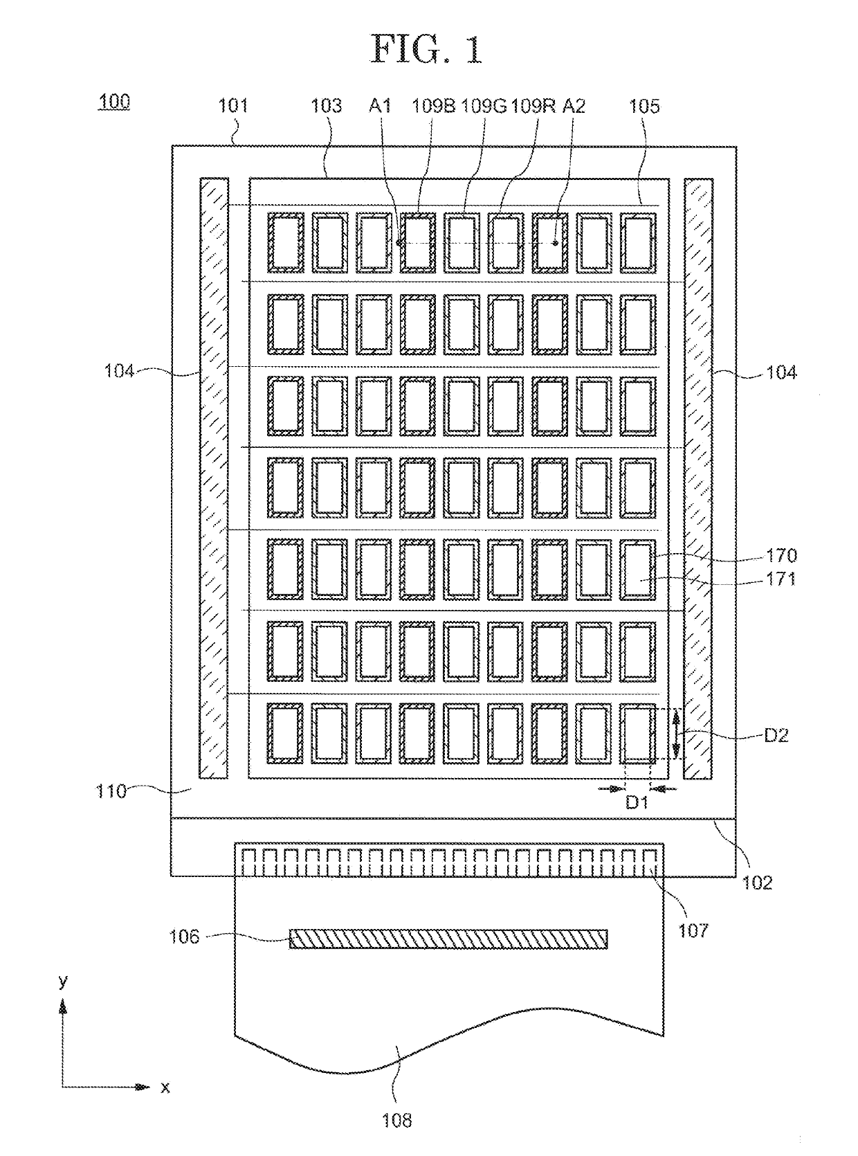
[0053]FIG. 1 is a schematic diagram showing a structure of a display device 100 according to one embodiment of the present invention. In addition, a schematic structure in the case when the display device 100 is viewed in planar view is shown in FIG. 1. In the present specification and the like, a state in which the display device 100 is viewed from a perpendicular direction to the screen (display part) is called a “planar view”.

[0054]The display device 100 includes a display part 103 formed above an insulating surface, a scanning signal line drive circuit 104, and a driver IC 106. In addition, an opposing substrate 102 is arranged above the displ...

second embodiment

3. Second Embodiment

[0097]In the embodiment, an example in which the shape of a part of the pixel electrode which is exposed by the opening part is different from the first embodiment is explained while referring to FIG. 15(A) to FIG. 15(F). The explanation of the background of the invention and the structure similar to that of the first embodiment may be omitted.

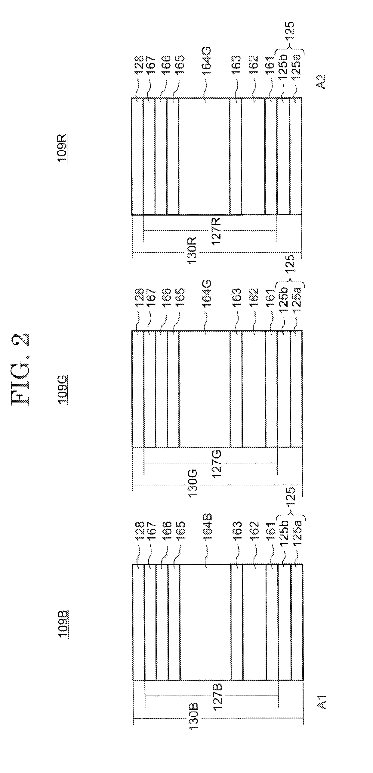
[0098]FIG. 1 shows an example in which the shape of a part 171 of the pixel electrode which is exposed by the opening part 170 is a rectangle. The shape of the part 171 of the pixel electrode which is exposed by the opening part 170 in the present embodiment is shown in FIG. 15(A) to FIG. 15(F). The shape of the part 171 of the pixel electrode which is exposed by the opening part 170 shown in FIG. 15(A) is a circular shape. The shape of the part 171 of the pixel electrode which is exposed by the opening part 170 shown in FIG. 15(B) to FIG. 15(F) is a polygonal shape. Specifically, the shape of the part 171 of the pixel elec...

third embodiment

4. Third Embodiment

[0102]In the present embodiment, a display device which is different from the first embodiment is explained while referring to FIG. 17 and FIG. 18. Furthermore, an explanation of the background of the invention and the same structure as in the first embodiment and the second embodiment may be omitted.

[0103]Generally, as explained in FIG. 4 and FIG. 5, the organic EL display device includes a light emitting element 130R, a light emitting element 130G and a light emitting element 130B. The light emitting layer 164R included in the light emitting element 130R, the light emitting layer 164G included in the light emitting element 130G and the light emitting layer 164B included in the light emitting element 130B are each formed using different materials. The light emitting element 130R, the light emitting element 130G and the light emitting element 130B are made from materials which are appropriately examined for light emitting efficiency, a voltage to be applied and li...


PUM


Abstract

A display device including a light emitting element including a first electrode, a light emitting layer and a plurality of organic layers including a hole transport layer above the first electrode, and a second electrode above the plurality of organic layers, and an insulation layer having an opening part exposing a part of the first electrode and covering a periphery side part of the first electrode, wherein when a hole mobility of the light emitting layer is μh1 and a hole mobility of the hole transport layer is μh2 thenμh2μh1≦103and when a periphery length of the part of the first electrode exposed by the opening part is L and an area of the first electrode exposed by the opening part is S0 thenLS0≧0.07

Description

CROSS REFERENCE TO RELATED APPLICATIONS[0001]This application is based upon and claims the benefit of priority from the prior Japanese Patent Application No. 2018-039999, filed on Mar. 6, 2018, the entire contents of which are incorporated herein by reference.FIELD[0002]An embodiment of the present invention is related to a display device.BACKGROUND[0003]An organic EL display device (Organic Electroluminescence Display) is known as one type of display device. In the organic EL display device, an organic electroluminescence material (organic EL material) is used in a light emitting element (organic EL element) which is included in each pixel of a display part. Unlike a liquid crystal display device or the like, an organic EL display device is a so-called self-light emitting type display device which realizes display by making an organic EL material emit light.[0004]In an organic EL display device, each light emitting element generally has an organic layer including a light emitting l...

Claims


Application Information

Patent Timeline
IPC IPC(8): H01L51/50H01L27/32H01L51/52
CPCH01L51/5209H01L51/5092H01L27/3246H01L51/5096H01L51/5221H01L51/5072H01L51/5056H01L27/3211H10K59/35H10K59/122H10K50/15H10K50/11H10K50/813H10K2101/00H10K50/16H10K50/18H10K50/82H10K50/171
Inventor UEMURA, TSUYOSHI
Owner JAPAN DISPLAY INC
Why Eureka
Try Eureka