Photonic device comprising a laser optically connected to a silicon waveguide and method for manufacturing such a photonic device

a photonic device and silicon waveguide technology, applied in the field of optoelectronic and photonic devices, can solve the problems of not being able to provide a dfb laser,

Active Publication Date: 2019-09-12
COMMISSARIAT A LENERGIE ATOMIQUE ET AUX ENERGIES ALTERNATIVES
View PDF0 Cites 10 Cited by
  • Summary
  • Abstract
  • Description
  • Claims
  • Application Information

AI Technical Summary

Benefits of technology

[0090]Such a step of forming the gain structure makes it possible to provide a gain structure parti

Problems solved by technology

Thus, on account of these dimensioning constraints, it is not possible with the usual configuration of a photonic device, such as that proposed by S. Keyvaninia and his co-authors, to provide a DFB laser having both a gain structure with a considerable length and a relatively low thickness of the first dielectric layer 110, that is to say less than 100 nm.
Thus, even an optimisation of this ratio does not make it possible to provide a DFB laser having both a gain structure with a considerable length, that is to say gre

Method used


Image

  • Photonic device comprising a laser optically connected to a silicon waveguide and method for manufacturing such a photonic device
  • Photonic device comprising a laser optically connected to a silicon waveguide and method for manufacturing such a photonic device
  • Photonic device comprising a laser optically connected to a silicon waveguide and method for manufacturing such a photonic device

Examples


first embodiment

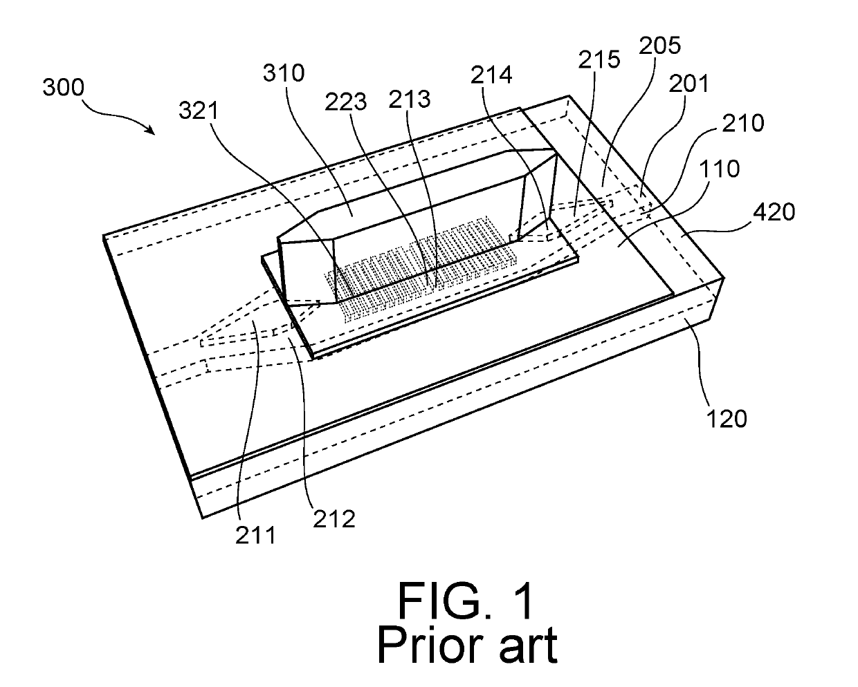
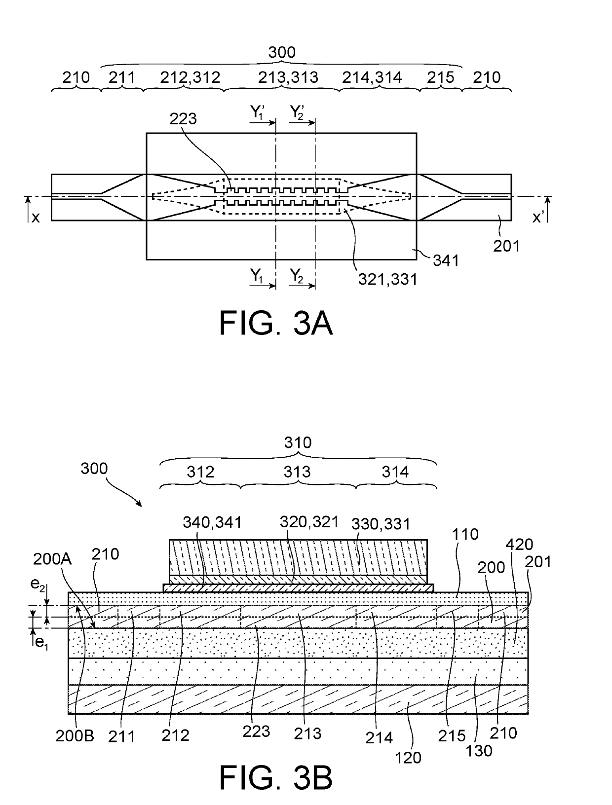
[0094]FIGS. 3A to 3D illustrate respectively a top view, a longitudinal sectional view, a transversal sectional view along a plane Y1Y1′ and a transversal sectional view along a plane Y2Y2′ of a photonic device according to the invention, the sectional planes Y1Y1′ and Y2Y2′ being shown in FIG. 3A

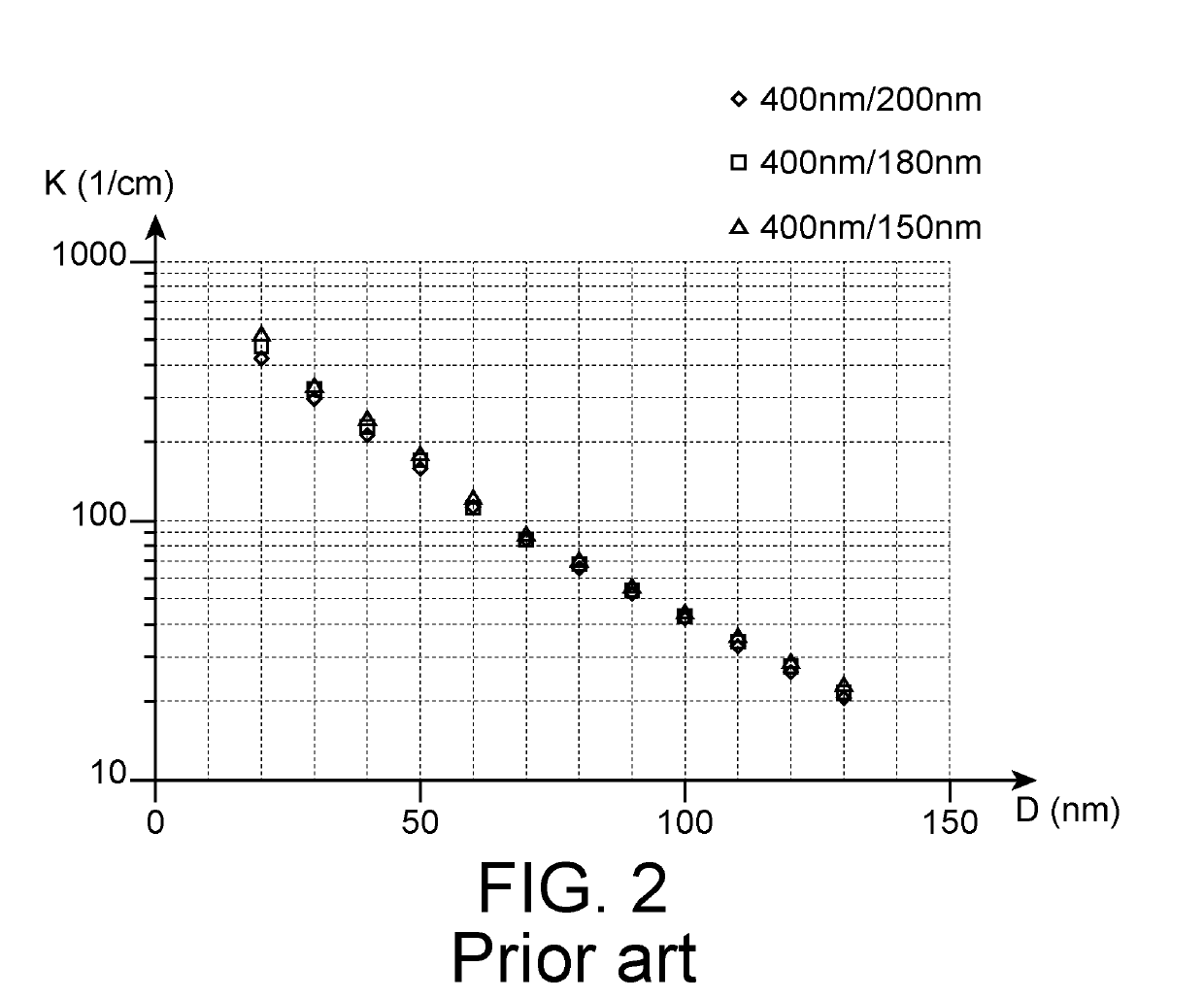
[0095]FIGS. 4A to 4D illustrate, for FIGS. 4A and 4B, transversal sectional views of a laser hybrid waveguide of respectively the photonic device illustrated in FIGS. 3A to 3D and a photonic device according to the prior art, the thickness of a silicon layer being identical for these two optical devices, and FIGS. 4C and 4D graphically representing the variation in the Kappa value of a Bragg grating of respectively the optical device of FIG. 4C and that of FIG. 4D, as a function of the widths of the wide ridges and narrow ridges,

[0096]FIGS. 5A to 5F illustrate, in longitudinal sectional views, the main steps for manufacturing a photonic device as illustrated in FIGS. 3A to 3F,

[0097]FIG. 6A ...

second embodiment

[0098]FIGS. 7A and 7B illustrate respectively a top view and a longitudinal sectional view of a device in which a gain structure of the photonic device has a first and a second end including a constant transversal section,

third embodiment

[0099]FIGS. 8A to 8B illustrate respectively a top view, a longitudinal sectional view, a transversal sectional view along a plane Y1Y1′ and a transversal sectional view along a plane Y2Y2′ of a photonic device in which a pattern of a third waveguide section has over a first thickness an alternation between a transversal section of a first width and a transversal section of a second width of zero value, the sectional planes Y1Y1 and Y2Y2′ being shown in FIG. 7A,

[0100]FIGS. 9A to 9E illustrate, in longitudinal sectional views, the main steps for manufacturing a photonic device as illustrated in FIGS. 7A to 7D,


PUM


Abstract

A photonic device comprising: a support; an intermediate layer (; an optical guiding level including a waveguide and a first to a fifth waveguide section. The photonic device further includes a first dielectric layer covering the optical guiding level and a gain structure in contact with the first dielectric layer. The second and fourth waveguide sections and the first and second ends of the gain structure form a first and a second zone of optical transition between a laser hybrid waveguide, and respectively the first and the fifth waveguide sections. A pattern forming a Bragg grating is arranged over a first part of the thickness of the third waveguide section which is away from the gain structure.

Description

CROSS-REFERENCE TO RELATED APPLICATIONS[0001]This application claims priority from French Patent Application No. 1852120 filed on Mar. 12, 2018. The content of this application is incorporated herein by reference in its entirety.TECHNICAL FIELD[0002]The invention relates to the field of optoelectronic and photonic devices.[0003]More specifically, the subject matter of the invention is a photonic device comprising a waveguide intended to accommodate several silicon photonic components and a hybrid laser on silicon including a gain medium capable of emitting light.PRIOR ART[0004]The manufacture of hybrid photonic devices integrating silicon photonic components and at least one hybrid laser on silicon including a gain medium capable of emitting light, such as a gain medium made of III-V semiconductor materials, must necessarily take into account design constraints as regards the dimensioning of the first silicon waveguide accommodating the silicon photonic components and the second sil...

Claims


Application Information

Patent Timeline
IPC IPC(8): H01S5/10H01S5/042H01S5/125G02B6/12G02B6/13H01S5/12
CPCG02B6/13H01S5/0422G02B2006/12121G02B6/12004H01S5/1032H01S5/125H01S5/12H01S5/026H01S5/20H01S5/34H01S5/021H01S5/0218H01S5/0265
Inventor MENEZO, SYLVIETHIESSEN, TORREY
Owner COMMISSARIAT A LENERGIE ATOMIQUE ET AUX ENERGIES ALTERNATIVES
Why Eureka
Try Eureka