

Compensation device for compensating pvt variations of an analog and/or digital circuit
- Summary
- Abstract
- Description
- Claims
- Application Information
AI Technical Summary
Benefits of technology
Problems solved by technology
Method used
Image

Examples
Embodiment Construction
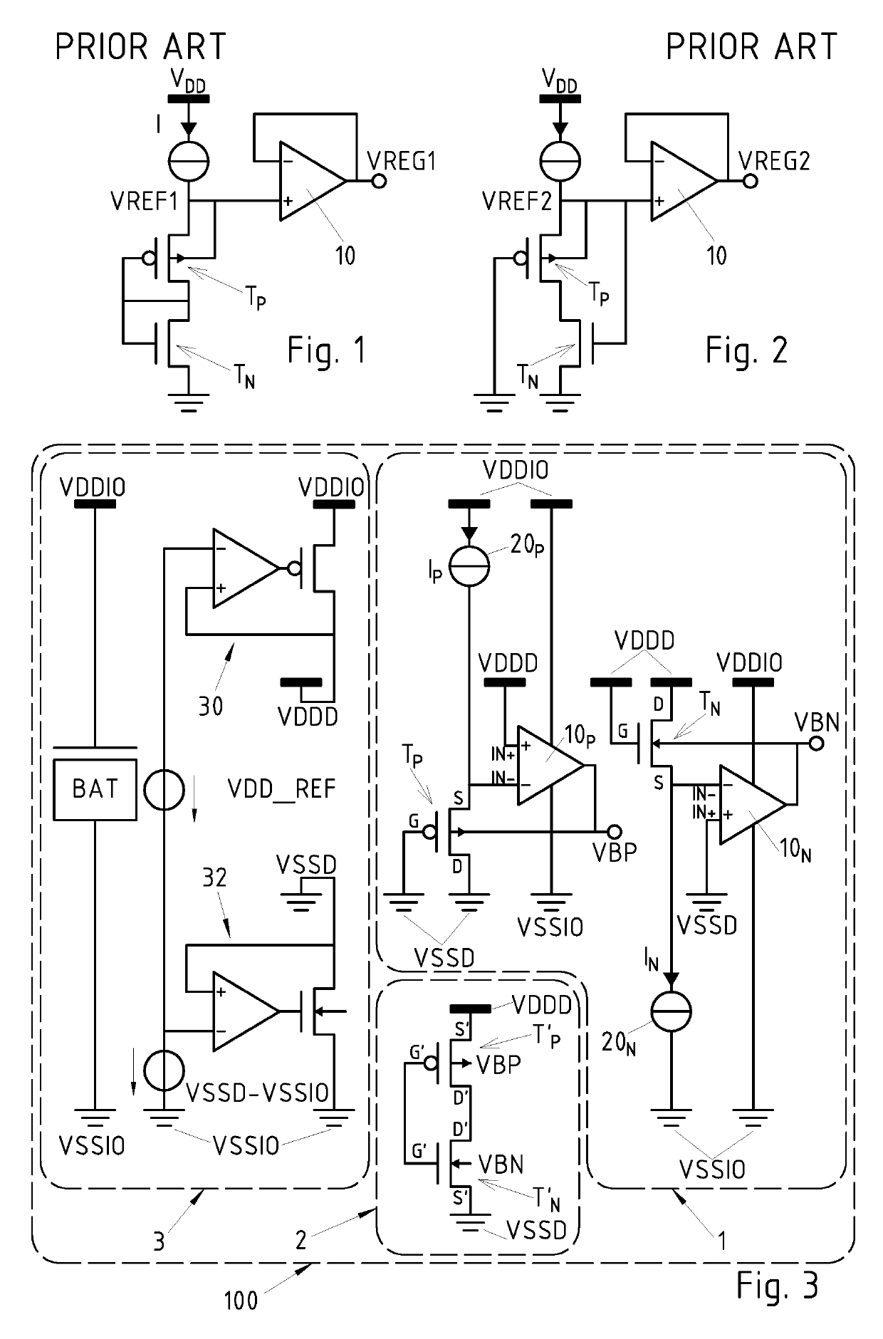
[0096]FIG. 3 shows a schematic view of the electronic device 100 according to an embodiment of the invention. In the illustrated embodiment it comprises:[0097]a compensation device 1, for compensating PVT variations of an analog and / or digital circuit 2,[0098]the analog and / or digital circuit 2,[0099]an input / output circuit 3.
[0100]Examples of analog and / or digital circuits 2 to be compensated comprise, but are not limited to, voltage or current references, amplifier, oscillator, memory cells (e.g. SRAM or ROM cells), digital accelerators, processors, etc.
[0101]In the illustrated embodiment the input / output circuit 3 comprising a battery BAT, arranged for generating a voltage equal to VDDIO−VSSIO, and means 30, 32 (two LDOs in this case) arranged for generating the voltages of supply source VDDD and of the supply source VSSD of the compensation device 1 and of the analog and / or digital circuit 2. However it must be understood that other means, as DCDC converters, can be used instead...
PUM
 Abstract
Description
Claims
Application Information