Semiconductor device

a technology of semiconductor devices and impurity concentrations, applied in semiconductor devices, semiconductor/solid-state device details, diodes, etc., can solve the problems of difficult to accurately control the impurity concentration or the cell pitch, and other properties (e.g., recovery properties) may be restricted, so as to improve recovery properties, secure the charge balance, and ensure the charge balance.

Active Publication Date: 2019-10-03
ROHM CO LTD
View PDF0 Cites 2 Cited by
  • Summary
  • Abstract
  • Description
  • Claims
  • Application Information

AI Technical Summary

Benefits of technology

[0006]An object of the present invention is to provide a semiconductor device which is capable of readily controlling the charge balance between a semiconductor layer and a column layer.
[0007]Another object of the present invention is to provide a semiconductor device which is capable of both securing the charge balance between a semiconductor layer and a column layer and improving the recovery property.

Problems solved by technology

However, it is difficult to accurately control the impurity concentration or the cell pitch, and as a result of placing a high priority on securing the charge balance, other properties (e.g., recovery property) may be restricted.

Method used


Image

  • Semiconductor device
  • Semiconductor device
  • Semiconductor device

Examples


Embodiment Construction

[0033]Hereinafter, referring to the attached drawings, the preferred embodiment of the present invention will be described below in more detail.

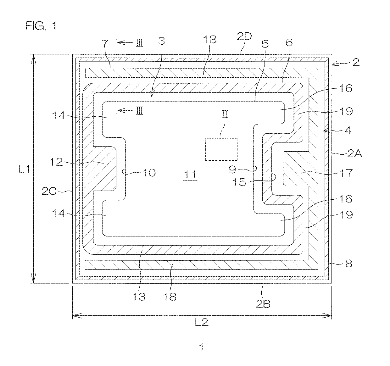
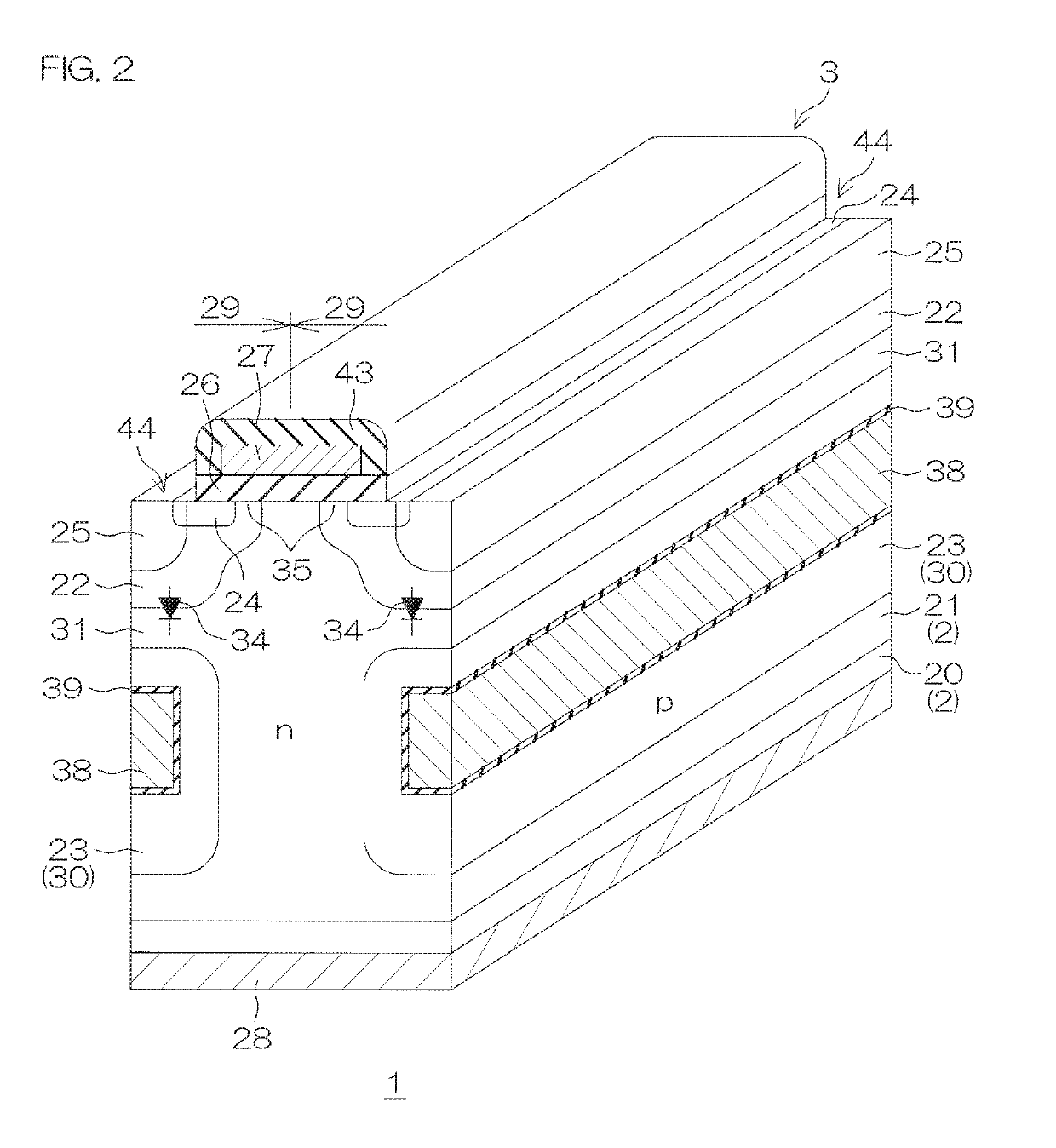
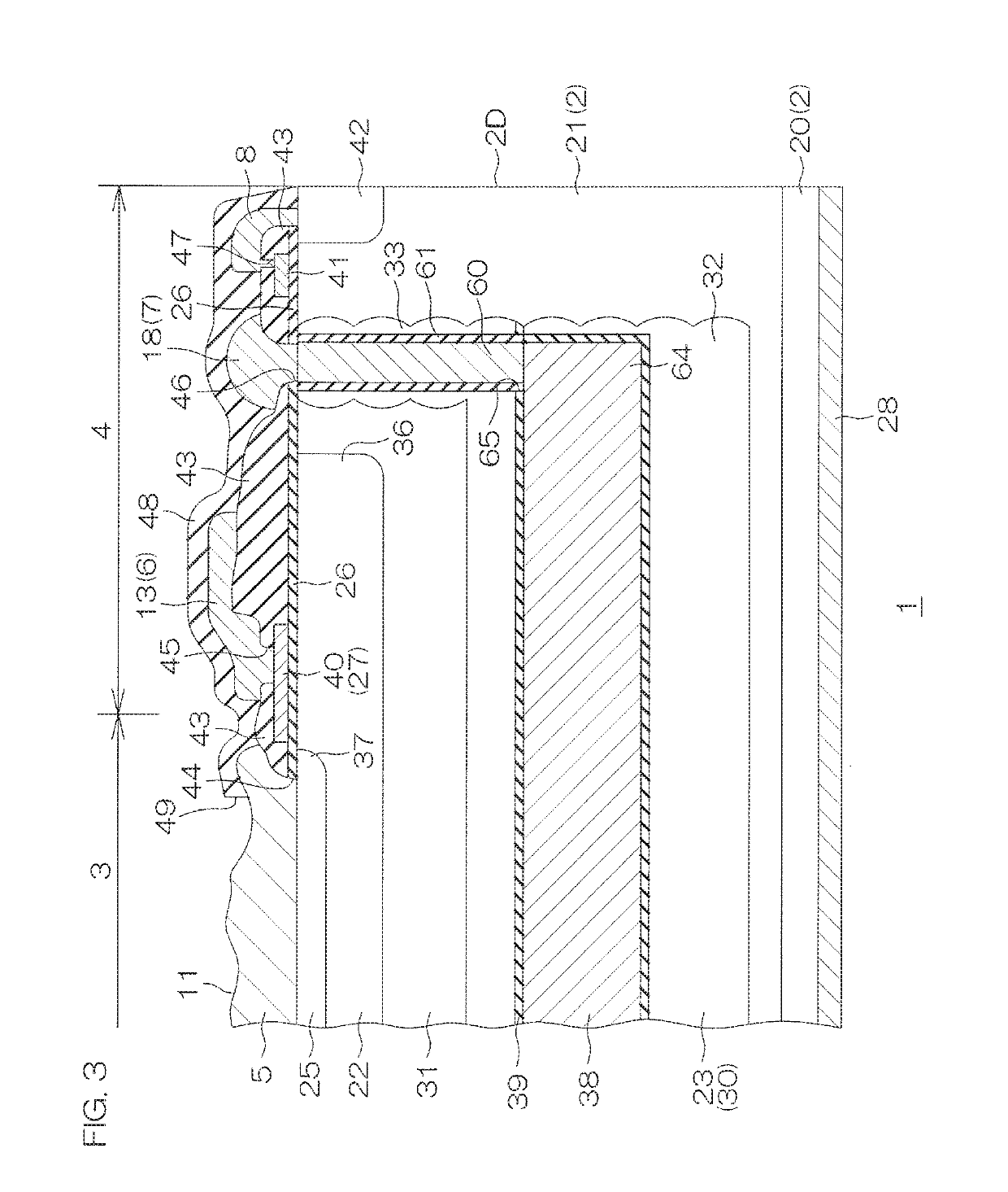
[0034]FIG. 1 is a schematic plan view illustrating a semiconductor device 1 according to a preferred embodiment of the present invention. Note that, in FIG. 1, for the sake of clarity, electrode films 5 to 8 are hatched for illustration.

[0035]The semiconductor device 1 includes a semiconductor substrate 2 as an example of a quadrangular semiconductor layer of the present invention in a plan view. The semiconductor substrate 2 may have a length L1 of, e.g., 1.0 mm to 9.0 mm in a first direction (in FIG. 1, a length along a side 2A or 2C of the semiconductor substrate 2) and a length L2 of, e.g., 1.0 mm to 9.0 mm in a second direction orthogonal to the first direction (in FIG. 1, a length along a side 2B or 2D of the semiconductor substrate 2).

[0036]In a plan view, the semiconductor substrate 2 includes an active portion 3 in the central area....


PUM


Abstract

A semiconductor device includes: a semiconductor layer of a first conductive type having a first surface and a second surface opposite to the first surface; a body region of a second conductive type selectively formed on the first surface of the semiconductor layer; a source region of the first conductive type formed inside the body region; a gate electrode opposing part of the body region via a gate insulating film; a column layer of the second conductive type formed at the second surface side with respect to the body region; an embedded electrode embedded in the column layer such that the embedded electrode is electrically isolated from the column layer; and a first electrode electrically connected to the embedded electrode.

Description

CROSS-REFERENCE TO RELATED APPLICATIONS[0001]The present application relates to Japanese Patent Application No. 2018-064794 filed with Japan Patent Office on Mar. 29, 2018, the entire disclosure of which is hereby incorporated by reference.TECHNICAL FIELD[0002]The present invention relates to a semiconductor device that includes a High Electron Mobility Transistor (HEMT).BACKGROUND ART[0003]Patent Literature 1 (WO 2010 / 024433) discloses a semiconductor device which includes: a first base layer; a drain layer provided on a rear surface of the first base layer; a second base layer formed on a surface of the first base layer; a source layer formed on a surface of the second base layer; a gate insulating film disposed on surfaces of the source layer and the second base layer; a gate electrode disposed on the gate insulating film; a column layer formed to oppose the drain layer in the first base layer below the second base layer and the source layer; a drain electrode provided on the dra...

Claims


Application Information

Patent Timeline
Patent Type & Authority Applications(United States)
IPC IPC(8): H01L29/78H01L29/06H01L29/40H01L29/10H01L29/36H01L29/16H01L29/08H01L29/66
CPCH01L29/0696H01L29/0634H01L29/0847H01L29/1033H01L29/36H01L29/407H01L29/66666H01L29/16H01L29/7827H01L29/7802H01L29/1095H01L23/4824H01L29/7811H01L29/0619H01L29/7805H01L2224/0603
Inventor KUBO, YUSUKE
Owner ROHM CO LTD
Why Eureka
Try Eureka