Protection of a gamma radiation detector
a gamma radiation detector and protection technology, applied in the field of gamma radiation detectors, can solve the problems of reducing the duration of such an intermittent imaging procedure, obviating the need for saturation recovery time, and absorbing stray x-ray quanta that are not absorbed in the x-ray detector, so as to improve the image quality of subsequently reconstructed images
- Summary
- Abstract
- Description
- Claims
- Application Information
AI Technical Summary
Benefits of technology
Problems solved by technology
Method used
Image
Examples
first embodiment
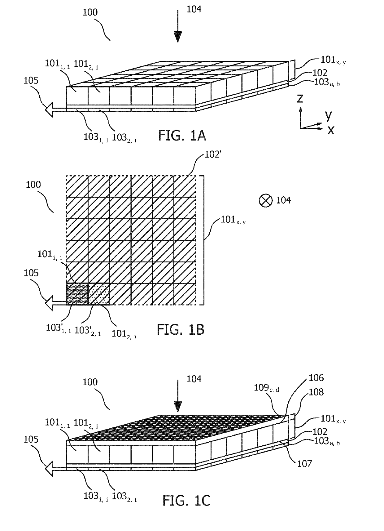
[0029]FIG. 1A illustrates a gamma radiation detector 100 that includes gamma scintillator array 101x, y, optical modulator 102, and first photodetector array 103a, b. Corresponding FIG. 1B illustrates the gamma radiation detector 100 of FIG. 1A as a plan view of the x-y plane, and in which the cross sectional area 102′ of a pixel of optical modulator 102 is highlighted by the hatched region. Gamma scintillator array 101x, y in FIG. 1A includes a plurality of first scintillator elements such as 1011, 1 and 1012, 1 that are suitable for generating scintillation light, termed herein “first scintillation light”, in response to received gamma quanta. First photodetector array 103a, b is suitable for detecting the first scintillation light generated by the gamma scintillator array. As illustrated in FIG. 1A, gamma scintillator array 101x, y, optical modulator 102 and first photodetector array 103a, b are arranged in a stacked configuration along gamma radiation receiving direction 104. Th...
second embodiment
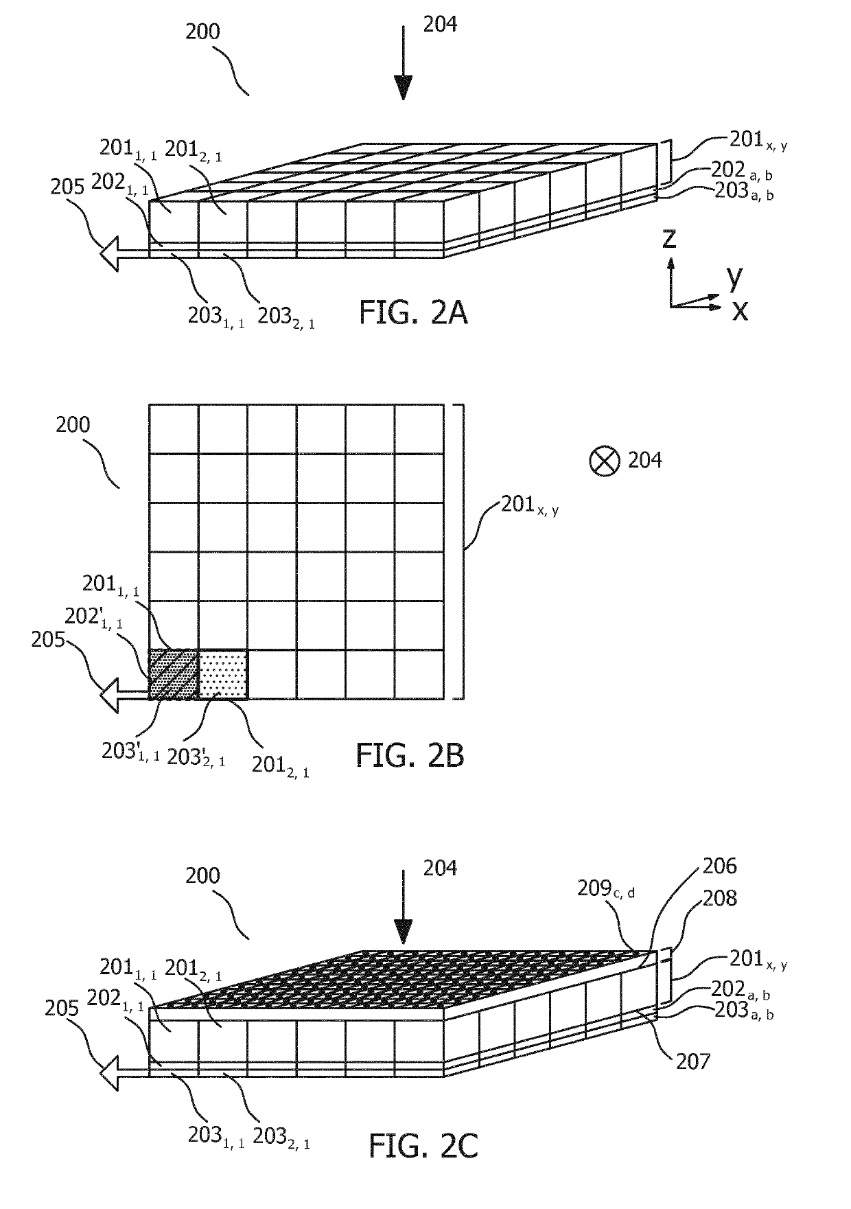
[0035]In FIG. 1 the cross sectional area of each scintillator element 101x, y in a plane that is perpendicular to the gamma radiation receiving direction 104 was illustrated as being equal to the cross sectional area of each photodetector pixel 103′a, b, however other arrangements are also suitable, for example the cross sectional area of each scintillator element 101x, y may alternatively be less than, or even greater than the cross sectional area of each photodetector pixel 103′a, b. Moreover the cross sectional area of optical modulator 102, i.e. 102′, in a plane that is perpendicular to the gamma radiation receiving direction 104, was illustrated as being greater than the cross sectional area of each photodetector pixel 103′a, b. FIG. 2A illustrates a gamma radiation detector 200 that includes gamma scintillator array 201x, y, optical modulator 202a, b, and first photodetector array 203a, b. Corresponding FIG. 2B illustrates the gamma radiation detector 200 of FIG. 2A as a plan ...
third embodiment
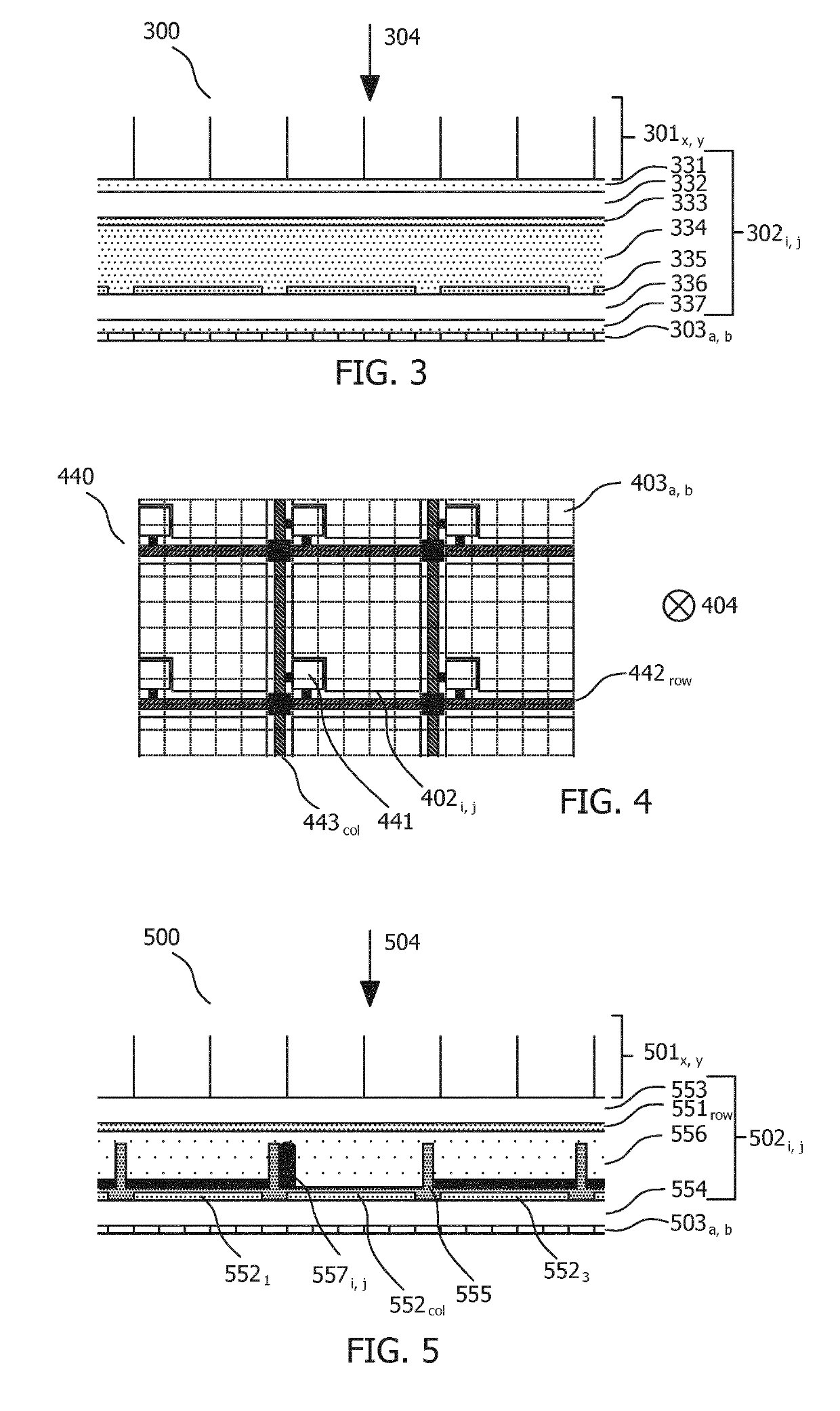
[0038]FIG. 3 illustrates third embodiment of a gamma radiation detector 300 in which an optical modulator is provided by a passive matrix liquid crystal array that includes a plurality of optical modulator pixels 302i, j. The Figure shows a cross section of the x-y plane illustrated in FIG. 1A. As mentioned above, in a preferred example the optical modulation is provided by a liquid crystal device. A liquid crystal device is preferred owing to the fast switching speeds available, high on-state transmission, and mature status of the technology. In FIG. 3 passive matrix liquid crystal array 302i, j is disposed between gamma scintillator array 301x, y and the first photodetector array 303a, b in order to modulate a transmission of the first scintillation light between the gamma scintillator array 301x, y and the first photodetector array 303a, b. Passive matrix liquid crystal array 302i, j may include a liquid crystal layer 334 disposed between glass plates 332, 336. Crossed polarizer ...
PUM
 Abstract
Description
Claims
Application Information


