Infiltration apparatus and methods of infiltrating an infiltrateable material

a technology of infiltration apparatus and infiltration method, which is applied in the direction of coating, chemical vapor deposition coating, metallic material coating process, etc., can solve the problems of high resolution polymer resists that may have a low etch resistance, high etch rate, and thin polymer resists

Pending Publication Date: 2019-12-05
ASM IP HLDG BV
View PDF8 Cites 231 Cited by
  • Summary
  • Abstract
  • Description
  • Claims
  • Application Information

AI Technical Summary

Problems solved by technology

However, such thin polymer resists may have several drawbacks.
In particular, high resolution polymer resists may have a low etch resistance, i.e., high etch rates.
This low etch resistance of the polymer resist makes the transfer of the patterned res...

Method used


Image

  • Infiltration apparatus and methods of infiltrating an infiltrateable material
  • Infiltration apparatus and methods of infiltrating an infiltrateable material
  • Infiltration apparatus and methods of infiltrating an infiltrateable material

Examples


Embodiment Construction

[0020]Although certain embodiments and examples are disclosed below, it will be understood by those in the art that the invention extends beyond the specifically disclosed embodiments and / or uses of the invention and obvious modifications and equivalents thereof. Thus, it is intended that the scope of the invention disclosed should not be limited by the particular disclosed embodiments described below.

[0021]The illustrations presented herein are not meant to be actual views of any particular material, structure, or device, but are merely idealized representations that are used to describe embodiments of the disclosure.

[0022]As used herein, the term “substrate” may refer to any underlying material or materials that may be used, or upon which, a device, a circuit, or a film may be formed.

[0023]As used herein, the term “infiltrateable material” may refer to any material into which an additional species, such as atoms, molecules, or ions, may be introduced.

[0024]As used herein, the term...


PUM


Abstract

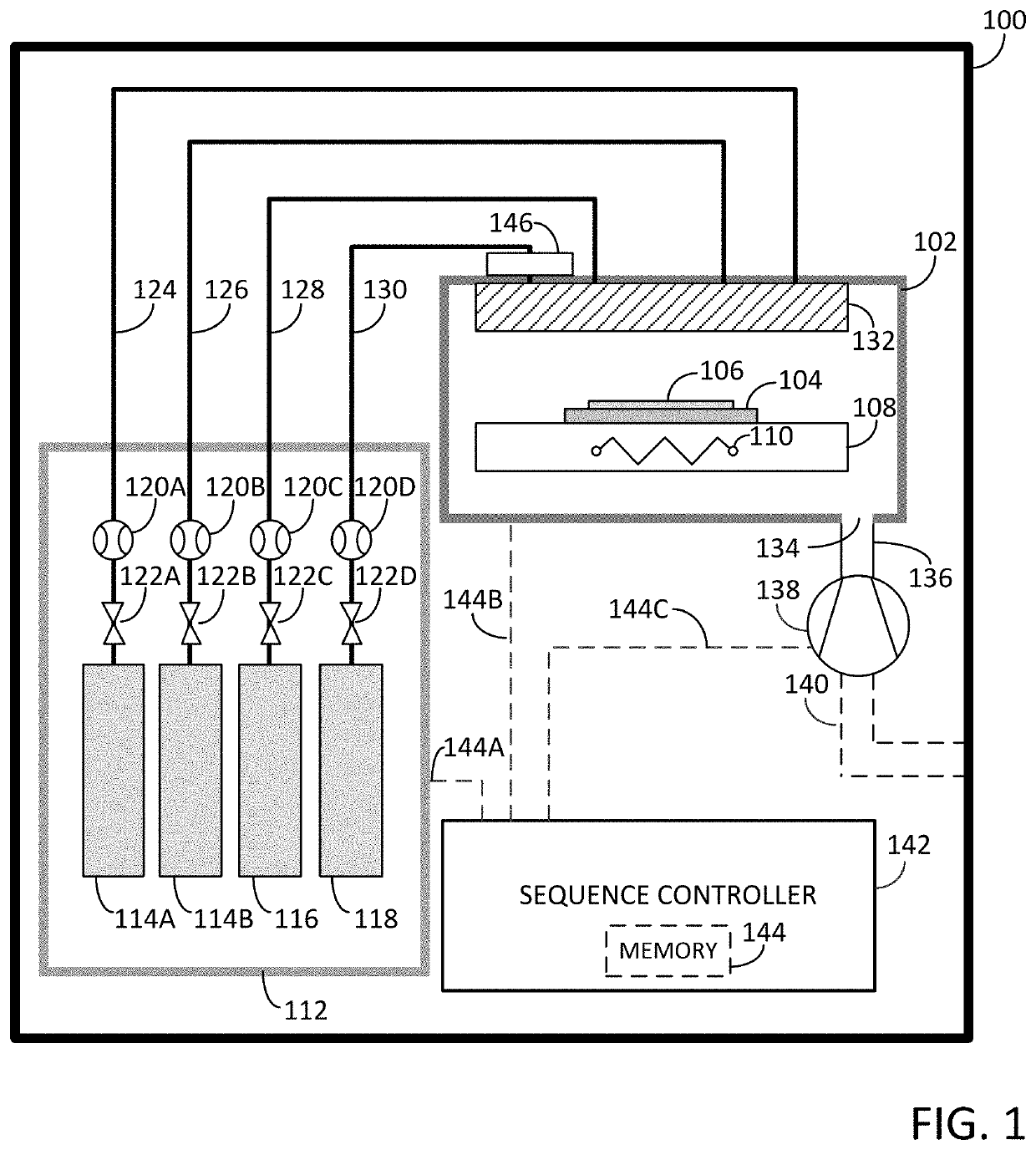
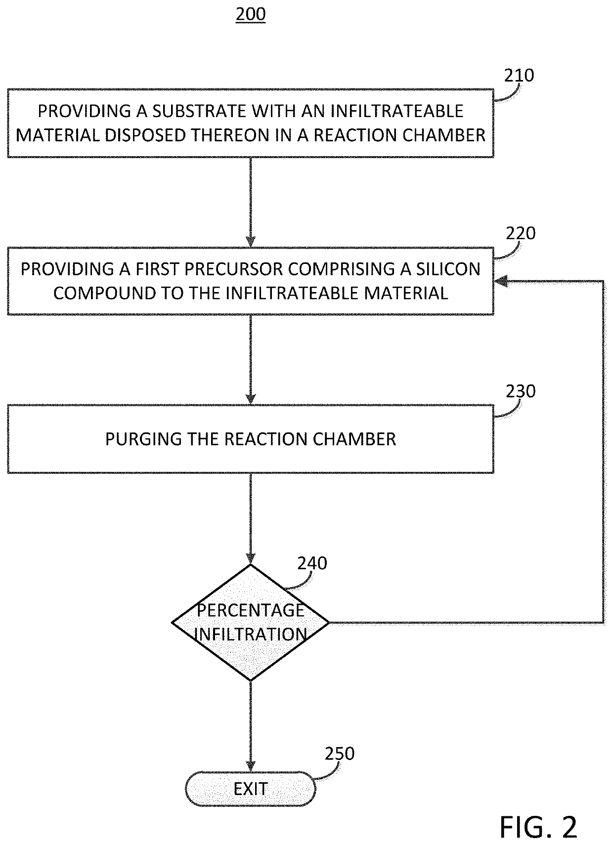
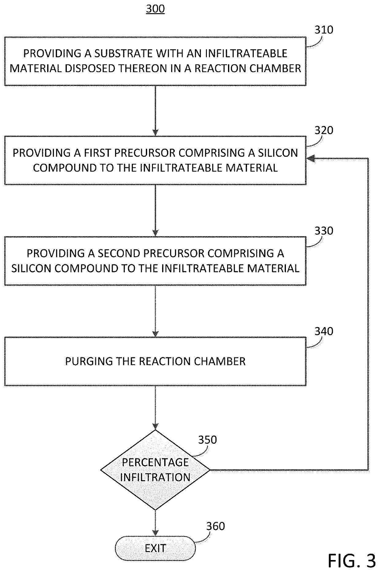
An infiltration apparatus is disclosed. The infiltration apparatus may include: a reaction chamber constructed and arranged to hold at least a substrate provided with an infiltrateable material thereon; a first precursor source constructed and arranged to provide a vapor a first precursor comprising a silicon compound; a precursor distribution system and removal system constructed and arranged to provide the reaction chamber with the vapor of the first precursor from the first precursor source and to remove the vapor of the first precursor from the reaction chamber; and a sequence controller operably connected to the precursor distribution system and removal system and comprising a memory provided with a program to execute infiltration of the infiltrateable material when run on the sequence controller by; activating the precursor distribution system and removal system to provide the vapor of the first precursor to the infiltrateable material on the substrate in the reaction chamber whereby the infiltrateable material on the substrate in the reaction chamber is infiltrated with silicon atoms by the reaction of the vapor of the first precursor with the infiltrateable material. Methods of infiltration and semiconductor device structure including infiltrated materials are also provided.

Description

FIELD OF INVENTION[0001]The present disclosure relates generally to an infiltration apparatus and particularly an infiltration apparatus configured for infiltrating an infiltrateable material with silicon atoms. The present disclosure also relates generally to methods of infiltrating an infiltrateable material.BACKGROUND OF THE DISCLOSURE[0002]As semiconductor device structures trend towards smaller and smaller geometries, different patterning techniques have arisen. These techniques include self-aligned multiple patterning, spacer defined quadruple patterning, deep ultraviolet lithography (DUV), extreme ultraviolet lithography, and DUV / EUV combined with spacer defined double patterning. In addition, direct self-assembly (DSA) has been considered as an option for future lithography applications.[0003]The patterning techniques described above may utilize at least one polymer resist disposed on a substrate to enable high resolution patterning of the substrate. To satisfy the requireme...

Claims


Application Information

Patent Timeline
IPC IPC(8): C23C16/455H01L21/027H01L21/02C23C16/56
CPCH01L21/0273C23C16/56H01L21/02211C23C16/45559C23C16/045C23C16/24C23C16/401C23C16/325C23C16/45523C23C16/45527
Inventor KACHEL, KRZYSZTOF KAMILFÄRM, ELINA
Owner ASM IP HLDG BV
Why Eureka
Try Eureka