Check patentability & draft patents in minutes with Patsnap Eureka AI!

Method for detecting defects in semiconductor device

a semiconductor device and defect detection technology, applied in semiconductor/solid-state device testing/measurement, image enhancement, instruments, etc., can solve the problems of noise in labelled image data, high cost, and large amount of image data in the fabrication defect detection process

Active Publication Date: 2020-01-30
SAMSUNG ELECTRONICS CO LTD
View PDF1 Cites 11 Cited by
  • Summary
  • Abstract
  • Description
  • Claims
  • Application Information

AI Technical Summary

Benefits of technology

The present patent discloses a method for detecting defects in a semiconductor device using a convolutional neural network (CNN). The method allows for accurate detection of defects in non-labeled image data or improperly labeled image data. The method involves training a normal CNN model and a label-noise CNN model using a sampled clean data set. The method also includes comparing the first prediction result with the second prediction result to perform noise correction when there is a label difference. The result is an improved accuracy of detecting defects in semiconductor devices.

Problems solved by technology

Unfortunately, manually labeling a large amount of image data in a fabrication defect detection process consumes much time and cost.
Further, even after the image data has been labeled, the labelled image data may include noise.

Method used


Image

  • Method for detecting defects in semiconductor device
  • Method for detecting defects in semiconductor device
  • Method for detecting defects in semiconductor device

Examples


Embodiment Construction

[0023]Hereinafter, example embodiments of the present disclosure will be described in detail with reference to the accompanying drawings.

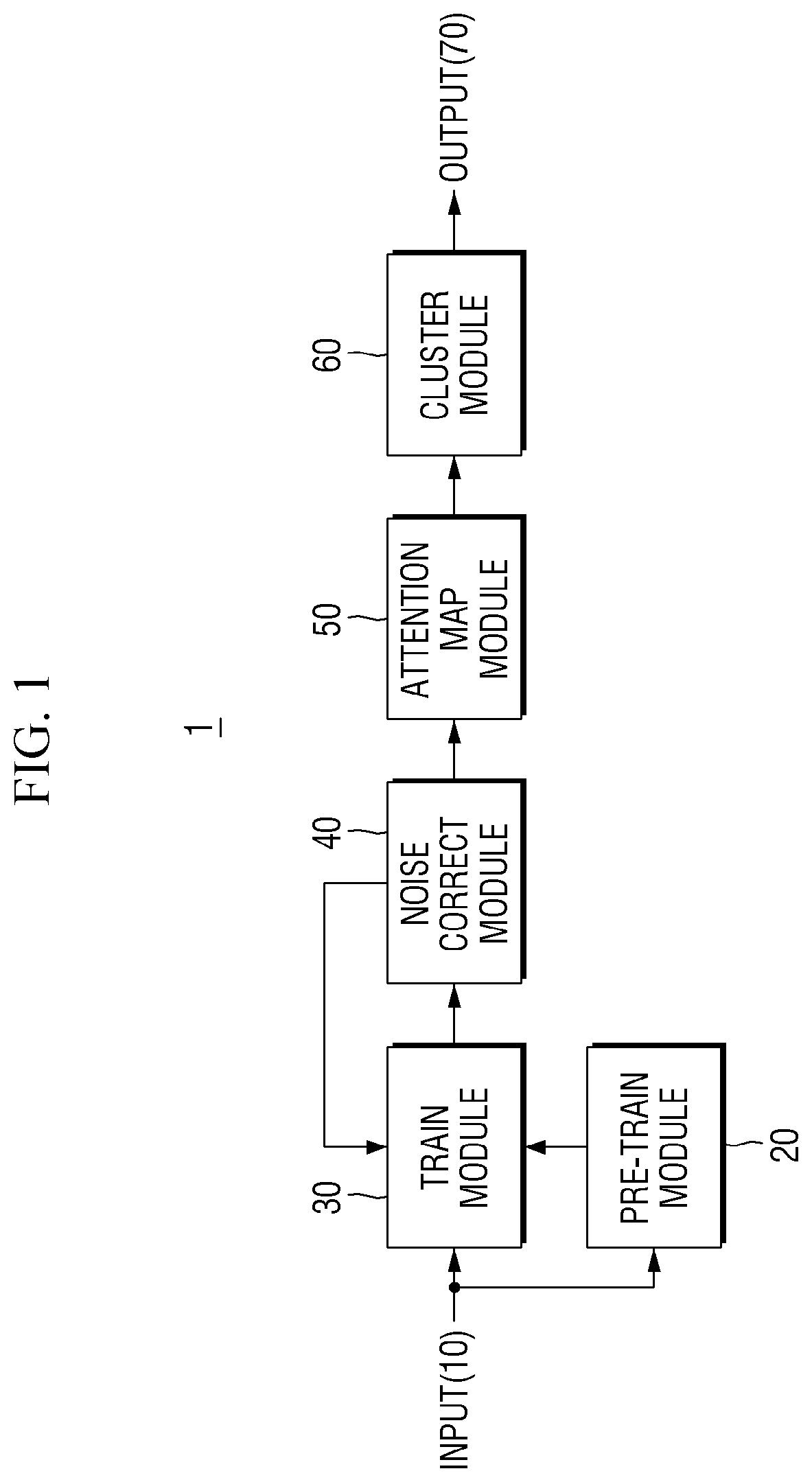
[0024]FIG. 1 is a block diagram for illustrating a defect detection system for a semiconductor device according to an example embodiment of the present disclosure.

[0025]Referring to FIG. 1, a defect detection system 1 for a semiconductor device according to an example embodiment of the present disclosure automatically detects defects occurring during the process of fabricating a semiconductor device by using machine learning, especially deep learning. Deep learning is a type of machine learning that is based on artificial neural networks. Neural networks are machine learning tools implemented by processors executing software and modeled after the human brain. Neural networks work by “learning” by incorporating new data. The defect detection system 1 improves the learning quality of neural networks that have levels becoming deeper by preprocessing l...


PUM


Abstract

A method for detecting defects in a semiconductor device includes pre-training a pre-trained convolutional neural network (CNN) model using a sampled clean data set extracted from a first data set; training a normal convolutional neural network model and a label-noise convolutional neural network model using first data of the first data set and the pre-trained convolutional neural network model. The method also includes outputting a first prediction result on whether second data of a second data set is good or bad using the second data and the normal convolutional neural network model; and outputting a second prediction result on whether second data is good or bad using the second data and the label-noise convolutional neural network model. The first prediction result is compared with the second prediction result to perform noise correction when there is a label difference. Third data created as results of the noise correction is added to the sampled clean data set. The normal convolutional neural network model and the label-noise convolutional neural network model are additionally using the sampled clean data set with the third data added.

Description

CROSS-REFERENCE TO RELATED APPLICATION[0001]This U.S. non-provisional patent application claims priority to Korean Patent Application No. 10-2018-0087488, filed on Jul. 27, 2018 in the Korean Intellectual Property Office, the disclosure of which is incorporated herein by reference in its entirety.BACKGROUND1. Field of the Disclosure[0002]The present disclosure relates to a method for detecting defects in semiconductor devices.2. Description of the Related Art[0003]Techniques for detecting defects occurring during a process of fabricating a semiconductor device are being used. In particular, in order to detect defects in a semiconductor device, techniques using machine learning such as artificial neural networks (ANNs) are attracting attention.[0004]In order to apply such techniques, a large amount of image data associated with the fabrication of semiconductor devices is required, along with labeling the image data to indicate whether the image data is good or bad. Unfortunately, man...

Claims


Application Information

Patent Timeline
IPC IPC(8): G06N3/04G06N3/08G06F17/50
CPCG06F30/30G06N3/08G06N3/0454G06T7/0004G06T2207/30148G06T2207/20081G06T2207/20084G06N3/045G06F18/23213H01L22/20G06N3/047G06T7/001G01N21/8803
Inventor HUH, INPARK, MIN CHULLEE, TAE HOJEONG, CHANG WOOKHWANG, CHAN YOUNG
Owner SAMSUNG ELECTRONICS CO LTD
Features
  • R&D
  • Intellectual Property
  • Life Sciences
  • Materials
  • Tech Scout
  • Unparalleled Data Quality
  • Higher Quality Content
  • 60% Fewer Hallucinations
Learn More