Memory arrangement and method for operating or testing a memory arrangement

a memory arrangement and memory technology, applied in the field of memory arrangement and method for operating or testing a memory arrangement, can solve the problems that failures of bit cells typically limit the lifetime of a memory arrangement, and achieve the effects of reducing reliability, reducing endurance cycles, and reducing failures

Active Publication Date: 2020-02-13
AMS AG
View PDF0 Cites 3 Cited by
  • Summary
  • Abstract
  • Description
  • Claims
  • Application Information

AI Technical Summary

Benefits of technology

[0050]In an embodiment, the memory arrangement performs a high efficient low cost EEPROM screening which enables area optimized dynamic byte error correction.
[0054]To extend the number of endurance cycle a byte replacement strategy is shown which may e.g. increase the number of endurance cycles by a factor of 20 with an area overhead in the range of 5% of the NVM memory plane.
[0056]The threshold voltages of well-produced NVM bit cells are showing a Gaussian distribution. If all bit cells are produced having lower reliability and therefore having less endurance cycles the erase of such cells takes place at a lower erase voltage which leads to a tail in the distribution of threshold voltages. Depending on the number of bit cells in the tail the endurance performance of the NVM memory can be predicted. Thus, weak bit cells can be screened out without stressing the NVM and therefore reducing the life time of the NVM due to test conditions.
[0057]A screening can be performed by testing the NVM with two or three different shorter erase pulses compared to the standard erase pulse. After each short test erase pulse the memory is readout with the sense amplifier arrangement. If a bit cell is already erased a bit replacement algorithm is used to overcome the early endurance fails. The exact number where the bit cell will fail cannot be predicted but by replacing the weak bit cells the number of endurance cycle stated in the datasheet may be achieved.

Problems solved by technology

Failures of bit cells typically limit the lifetime of a memory arrangement.

Method used


Image

  • Memory arrangement and method for operating or testing a memory arrangement
  • Memory arrangement and method for operating or testing a memory arrangement
  • Memory arrangement and method for operating or testing a memory arrangement

Examples


Embodiment Construction

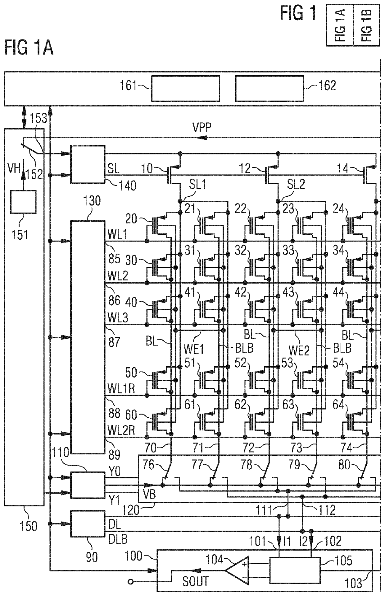
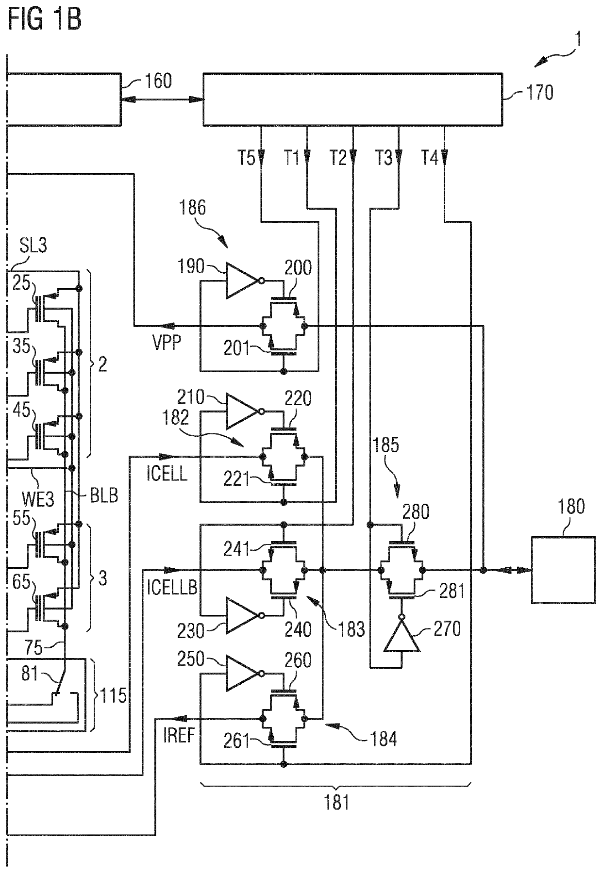
[0068]FIG. 1A shows an exemplary embodiment of a memory arrangement 1 comprising a non-volatile memory plane 2, a replacement plane 3, a y-decoder arrangement 115 and a sense amplifier arrangement 100. Both the non-volatile memory plane 2 and the replacement plane 3 are coupled via the y-decoder arrangement 115 to the sense amplifier arrangement 100. Non-volatile memory is shorted to NVM. A plane can also be called array. Thus, the non-volatile memory plane 2 can also be named non-volatile memory array. The replacement plane 3 can also be called replacement array. The NVM plane 2 comprises a first and a second bit cell 20, 21. The first bit cell 20 comprises a first memory transistor having a control terminal, a first and a second terminal and a substrate terminal. Correspondingly, the second bit cell 21 comprises a second memory transistor having a control terminal, a first and a second terminal and a substrate terminal. The first bit cell 20 is configured for non-volatile storage ...


PUM


Abstract

A memory arrangement comprises a non-volatile memory plane (2), a replacement plane (3), an address select block (302), and a counter arrangement (300) having at least one counter (310 to 312). The at least one counter (310 to 312) is configured to be incremented at a write cycle of the memory arrangement (1). The address select block (302) is configured to switch from the non-volatile memory plane (2) to the replacement plane (3), if a counter value of the at least one counter (310 to 312) is higher than a predetermined limit.

Description

CROSS-REFERENCE TO RELATED APPLICATIONS[0001]The present application is the national stage entry of International Patent Application No. PCT / EP2018 / 054836, filed on Feb. 27, 2018, which claims the benefit of priority of European Patent Application No. 17158340.4, filed on Feb. 28, 2017, all of which are hereby incorporated by reference in their entirety for all purposes.BACKGROUND OF THE INVENTION[0002]The present patent application is related to a memory arrangement, a method for operating a memory arrangement and a method for testing a memory arrangement.[0003]Memory arrangements often comprise non-volatile bit cells. The bit cells can withstand a high number of endurance cycles. Failures of bit cells typically limit the lifetime of a memory arrangement.SUMMARY OF THE INVENTION[0004]In an embodiment, a memory arrangement comprises a non-volatile memory plane, a replacement plane, an address select block and a counter arrangement having at least one counter. The at least one counte...

Claims


Application Information

Patent Timeline
Patent Type & Authority Applications(United States)
IPC IPC(8): G11C16/34G11C16/08G11C16/04G11C29/38
CPCG11C16/08G11C16/0483G11C16/3495G11C29/38G11C29/50004G11C2029/5006G11C29/76
Inventor SCHATZBERGER, GREGORLEISENBERGER, FRIEDRICH PETERSARSON, PETER
Owner AMS AG
Why Eureka
Try Eureka