

Semiconductor substrate manufacturing method
a semiconductor substrate and manufacturing method technology, applied in the direction of semiconductor/solid-state device testing/measurement, instruments, measurement devices, etc., can solve the problems of high intensity of light detected using pl evaluation methods, inability to accurately evaluate whether metal contamination is present in the semiconductor substrate and the degree of metal contamination, etc., to achieve accurate and easy evaluation, accurate and easy evaluation
Active Publication Date: 2020-02-27
SK SILTRON CO LTD
View PDF0 Cites 0 Cited by
- Summary
- Abstract
- Description
- Claims
- Application Information
AI Technical Summary
Benefits of technology
This semiconductor substrate manufacturing method can accurately and easily evaluate if a semiconductor substrate is contaminated with metal or the degree of metal contamination. It can do this for both lightly-doped and heavily-doped semiconductor substrates.
Problems solved by technology
In the convention PL evaluation method, however, surface recombination loss occurs due to external contamination of the semiconductor substrate and the processed state of the semiconductor substrate, whereby it is not possible to accurately evaluate whether the semiconductor substrate is contaminated or the degree of contamination.
Also, in the case in which the semiconductor substrate is doped at a high concentration, the intensity of light detected using the PL evaluation method is high, whereby it is not possible to accurately evaluate whether metal contamination is present in the semiconductor substrate and the degree of metal contamination.
Method used
View moreImage
Smart ImageViewing Examples

Examples
Embodiment Construction
[0129]Various embodiments have been described in the best mode for carrying out the invention.
INDUSTRIAL APPLICABILITY
[0130]A semiconductor substrate manufacturing method according to an embodiment may be used in the semiconductor substrate manufacturing field.
Login to View More PUM
| Property | Measurement | Unit |
|---|---|---|
| temperature | aaaaa | aaaaa |
| wavelength | aaaaa | aaaaa |
| wavelength | aaaaa | aaaaa |
Abstract
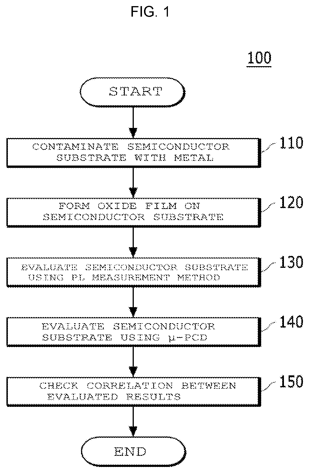
A semiconductor substrate manufacturing method according to an embodiment comprises the steps of: contaminating at least one of a surface layer of a doped semiconductor substrate having a specific resistance of less than 0.1 Ω·cm and a bulk layer below the surface layer with at least one metal of Fe, Cu, and Ni; performing dry oxidation at 950° C. for 30 minutes to forcibly form an oxide film on the surface of the semiconductor substrate; and assessing at least one of the presence and the degree of contamination of metal contained in at least one of the oxide film-formed surface layer and bulk layer by using a photoluminescence assessment method.
Description
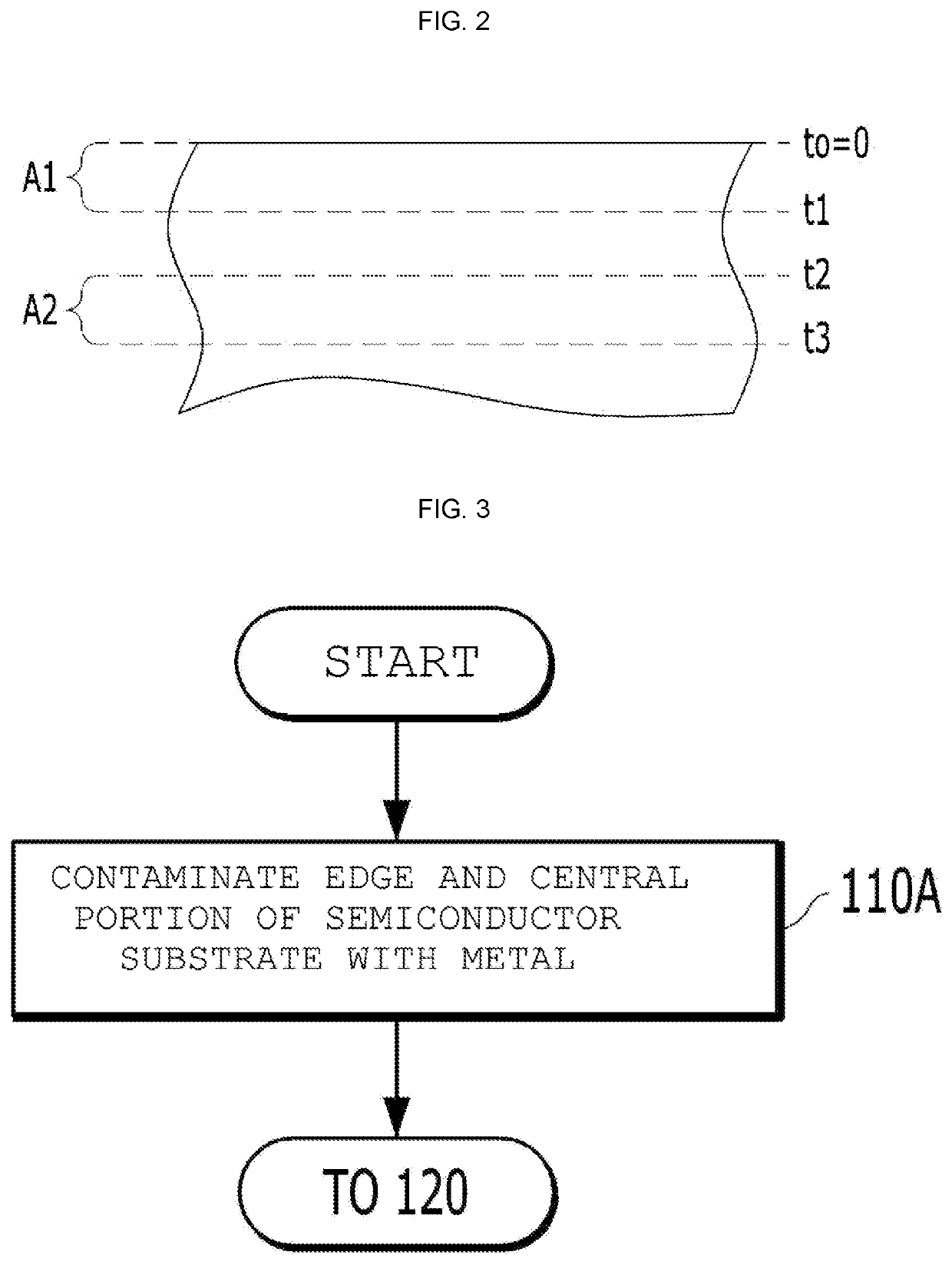
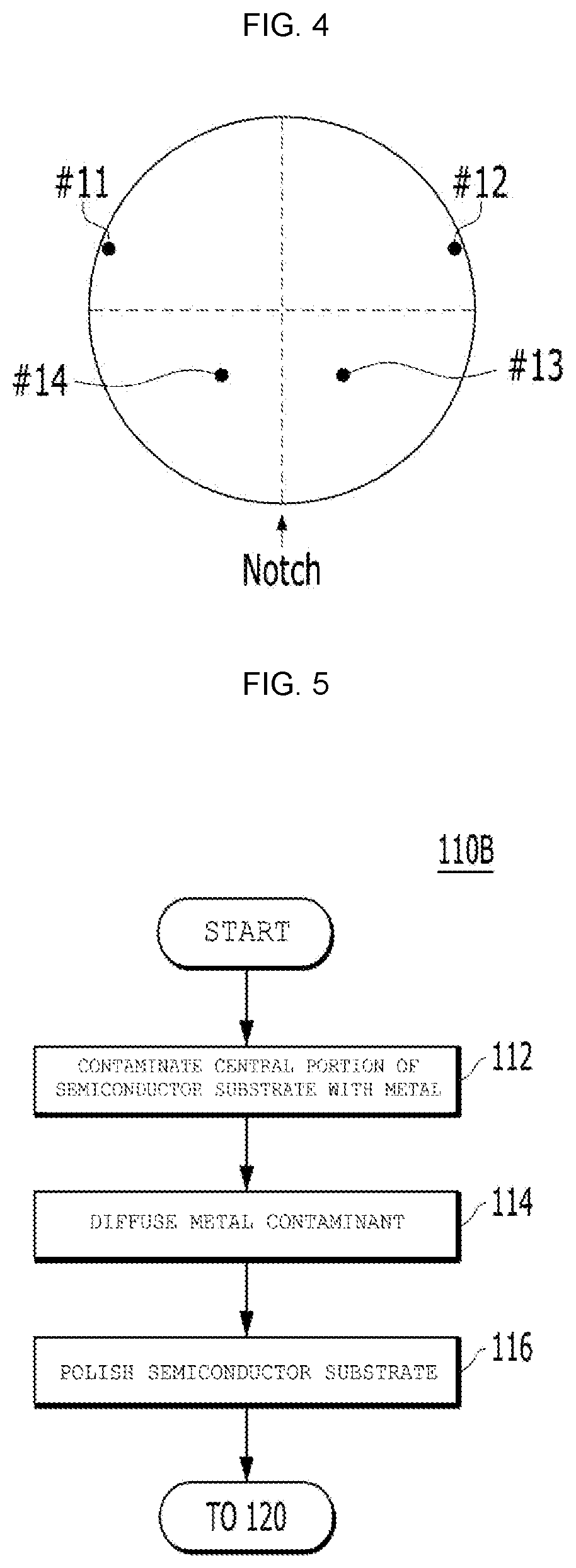
TECHNICAL FIELD[0001]Embodiments relate to a semiconductor substrate manufacturing method.BACKGROUND ART[0002]When a semiconductor substrate is manufactured, the result of evaluation of the semiconductor substrate may be usefully used. There is a photoluminescence (PL) evaluation method, as an example of a semiconductor substrate evaluation method. In the PL evaluation method, excitation light is radiated to the surface of a semiconductor substrate, and light generated when electron / hole pairs, excited by the excitation light, are recombined is detected in order to obtain information about the quality of the semiconductor substrate, for example, information about various crystalline defects, such as metal contamination or defects in the semiconductor substrate.[0003]In the convention PL evaluation method, however, surface recombination loss occurs due to external contamination of the semiconductor substrate and the processed state of the semiconductor substrate, whereby it is not po...
Claims
Login to View More Application Information
Patent Timeline
 Patent Type & AuthorityApplications(United States)
IPC IPC(8): H01L21/66H01L21/02H01L21/223H01L21/304H01L21/324
CPCH01L21/223H01L21/304H01L21/324H01L21/02043H01L22/12H01L21/02236H01L21/02554H01L21/0257G01N21/6489G01N21/9501H01L21/02005H01L21/3212H01L22/24
InventorLEE, KYUNG SUNHAM, HO CHAN
OwnerSK SILTRON CO LTD