Method and apparatus for testing semiconductor devices with preheating

a technology for semiconductor devices and preheating, which is applied in the direction of electronic circuit testing, measurement devices, instruments, etc., can solve the problem of time-consuming process of prior art methods, and achieve the effect of reducing the consumed time for heating the probe card

Inactive Publication Date: 2020-06-04
SPIROX INC
View PDF0 Cites 0 Cited by
  • Summary
  • Abstract
  • Description
  • Claims
  • Application Information

AI Technical Summary

Benefits of technology

[0007]An objective of the present invention is to provide method and apparatus for testing semiconductor devices with preheating, which heating a probe card and a plurality of pogo pins prior to installation for testing and heating the probe card to first default temperature, deforming the probe card and maintaining the temperature of the probe card during the testing process, for reducing the consumed time to heat the probe card again.

Problems solved by technology

The disadvantages of using the prior art's method is a time-consuming process, and after a device is tested completely, the test carrier has to move away to replace the device to be tested with a new device to test carrier.

Method used


Image

  • Method and apparatus for testing semiconductor devices with preheating
  • Method and apparatus for testing semiconductor devices with preheating
  • Method and apparatus for testing semiconductor devices with preheating

Examples


example 1

[0038]

TABLE 1The temperature ofThe temperature ofthe test carrierthe first heater1 85° C.32.5° C.~52.5° C.2100° C.40° C.~60° C.3125° C.52.5° C.~72.5° C.

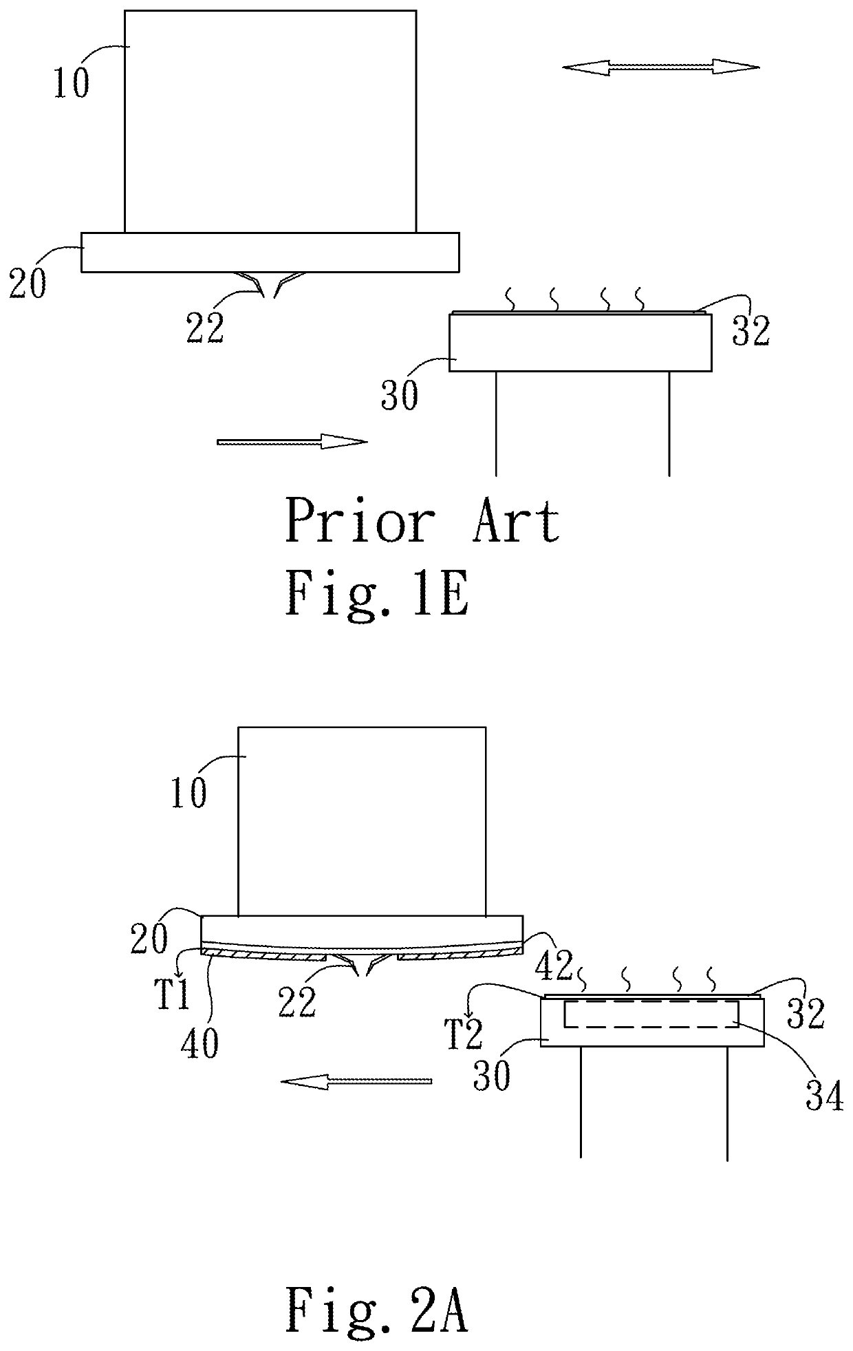
[0039]As shown in Table 1, when the actual temperature of the test carrier is 85° C., the actual temperature set on the first heater 40 to heat the probe card 20 would be balanced to only about 32.5° C.˜52.5° C., when the actual temperature of the test carrier 30 is 100° C., the actual temperature set on the first heater 40 to heat the probe card 20 would be higher to only about 40° C.˜60° C., and so and so forth. Thus, the first heater heats the probe card with half a temperature±10° C. of an actual temperature of the second heater 34. As a result of the movement of the test carrier 30 during the testing, the probe card 20 of the present invention will remain stable.

[0040]Referring to FIGS. 3A-C, they show a perspective view of how the first heater 40 is attached to the probe card 20 in accordance with another embodiment of the pres...


PUM

PropertyMeasurementUnit
temperatureaaaaaaaaaa

Abstract

Embodiments of method and apparatus for testing a semiconductor device with a probe card having a first heater underneath prior to testing are provided herein, for heating the probe card to a first default temperature to keep the. A test carrier is heated to a second default temperature

Description

FIELD OF THE INVENTION[0001]The present invention generally relates to method and apparatus for testing a device, in particular to method and apparatus for testing a semiconductor device, such as a wafer, with a preheating element.BACKGROUND OF THE INVENTION[0002]In recent years, Integrated circuits (ICs) are manufactured and tested in a wafer before being diced from the wafer and mounted in packages, modules, or directly on a printed circuit board. Wafer level IC testing is a critical part of the IC manufacturing process that identifies the ICs to judge if the ICs function properly and provides feedback for improving product design and reducing manufacturing cost. Wafer level IC testing also prevents non-functioning ICs from going through the cost of packaging and in some applications can be used for stress testing or burn-in testing at high temperature to screen ICs to assure long-term reliability.[0003]In the conventional wafer level IC testing, probe cards are used to provide an...

Claims


Application Information

Patent Timeline
Patent Type & Authority Applications(United States)
IPC IPC(8): G01R31/28G01R1/067G01R1/073
CPCG01R1/07342G01R31/2863G01R1/06722G01R31/2875
Inventor HUANG, TENG-CHUNGLEE, CHIH-CHIANG
Owner SPIROX INC
Why Eureka
Try Eureka