Manufacturing method of organic thin film transistor

a manufacturing method and organic technology, applied in the field of display technology, can solve the problems of low production capacity of display devices and increase production costs, and achieve the effects of reducing consumption time of manufacturing process, high quality, and large area

Active Publication Date: 2019-05-23
WUHAN CHINA STAR OPTOELECTRONICS TECH CO LTD
View PDF10 Cites 0 Cited by
  • Summary
  • Abstract
  • Description
  • Claims
  • Application Information

AI Technical Summary

Benefits of technology

[0027]The benefits of the present application are: the graphene layer is formed on the surface of the metal substrate in mass production. The organic semiconductor nano lines (monocrystalline semiconductor) are grown in mass production by graphene layer. The semiconductor layer having organic thin film transistors are formed after transferring the organic semiconductor nano lines on the target substrate. A large amount of the organic semiconductor nano lines can be formed at a time on the surface of the metal substrate with a large area. The transferring skills of roll-to-roll and roll-to-sheet are mutual and can transfer the organic semiconductor nano lines of the metal substrate on the target substrate in mass production rapidly and with high quality for reducing the consumed time of manufacture process and satisfying the requirement of mass production. The production capacity of display device is high and the production cost is reduced.

Problems solved by technology

On this account, the technical issue to be solved by the present application is to provide a manufacturing method of an organic thin film transistor to solve the issue that the fabrication of OTFT in prior art is limited by the production process and equipment, resulting in the inability to carry out large-scale production to lead to the low production capacity of the display devices and the increase in the production cost.

Method used


Image

  • Manufacturing method of organic thin film transistor
  • Manufacturing method of organic thin film transistor
  • Manufacturing method of organic thin film transistor

Examples


Embodiment Construction

[0034]Embodiments of the present application are described in detail with the technical matters, structural features, achieved objects, and effects with reference to the accompanying drawings as follows. It is clear that the described embodiments are part of embodiments of the present application, but not all embodiments. Based on the embodiments of the present application, all other embodiments to those of ordinary skill in the premise of no creative efforts obtained, should all be considered within the scope of protection of the present application.

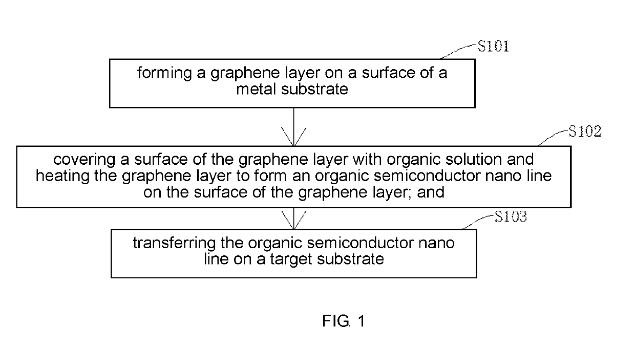
[0035]FIG. 1 is a flowchart of a manufacturing method of an organic thin film transistor provided by the embodiment of the present application. As show in figure, the manufacturing method of the organic thin film transistor provided by the embodiment of the present application comprises steps of:

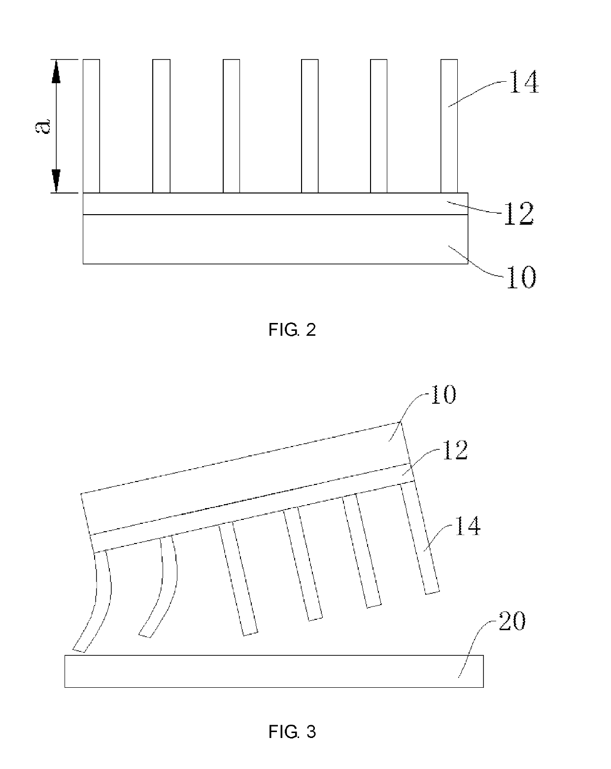
[0036]S101, forming a graphene layer 12 on a surface of a metal substrate 10.

[0037]In the present embodiment, the graphene layer 12 is formed o...


PUM

PropertyMeasurementUnit
lengthaaaaaaaaaa
thicknessaaaaaaaaaa
temperatureaaaaaaaaaa

Abstract

A method for manufacturing an organic thin film transistor includes steps of: forming a graphene layer on a surface of a metal substrate; covering a surface of the graphene layer with an organic solution and heating the graphene layer to form organic semiconductor nano lines on the surface of the graphene layer; and transferring the organic semiconductor nano lines to a target substrate. The graphene layer is formed on the surface of the metal substrate in mass production. The organic semiconductor nano lines (monocrystalline semiconductor) are grown in mass production by the graphene layer. The semiconductor layer having organic thin film transistors is formed after transferring the organic semiconductor nano lines on the target substrate. A large amount of the organic semiconductor nano lines can be formed simultaneously on the surface of the metal substrate with a large area.

Description

CROSS REFERENCE[0001]This is a continuation application of co-pending U.S. patent application Ser. No. 14 / 544,015, filed on Jul. 16, 2017, which is a national stage of foreign priority of PCT Application No. PCT / CN2017 / 082630, filed on Apr. 28, 2017, claiming foreign priority of Chinese Patent Application No. 201710245003.5, entitled “Manufacturing method of organic thin film transistor”, filed on Apr. 14, 2017, the disclosure of which is incorporated herein by reference in its entirety.FIELD OF THE INVENTION[0002]The present application relates to a display technology field, and more particularly to a manufacturing method of an organic thin film transistor.BACKGROUND OF THE INVENTION[0003]With the continuous progress of display technology, the flexible display device gradually appears in the market and the novel appearance of the flexible display device has a great attraction to the user. The Thin Film Transistors (TFT) are located on the array substrate of the flexible display dev...

Claims


Application Information

Patent Timeline
Patent Type & Authority Applications(United States)
IPC IPC(8): H01L51/05H01L27/32H01L51/00
CPCH01L51/0558H01L27/3274H01L51/0013H01L51/0052H01L51/0045H10K59/125H10K10/484H10K71/18H10K85/20H10K85/615
Inventor LIANG, BOWANG, WEI
Owner WUHAN CHINA STAR OPTOELECTRONICS TECH CO LTD
Why Eureka
Try Eureka