Carrier and Component with a Buffer Layer, and Method for Producing a Component

a buffer layer and carrier technology, applied in the direction of basic electric elements, electrical apparatus, semiconductor devices, etc., can solve problems such as mechanical fractures, and achieve the effect of improving mechanical stability, simplifying and efficien

Active Publication Date: 2020-07-23
OSRAM OLED
View PDF0 Cites 0 Cited by
  • Summary
  • Abstract
  • Description
  • Claims
  • Application Information

AI Technical Summary

Benefits of technology

[0004]Embodiments provide a temperature stable carrier and a component having increased mechanical stability. Further embodiments provide a simplified and efficient method for producing a mechanically and thermally stable component.

Problems solved by technology

The internal tensions can lead to damage, in particular to undesirable deformations of the component or of the semiconductor chip or of the carrier, as a result of which the deformations can cause mechanical fractures in the component or severe bend and finally delamination of the semiconductor chip from the carrier.

Method used


Image

  • Carrier and Component with a Buffer Layer, and Method for Producing a Component
  • Carrier and Component with a Buffer Layer, and Method for Producing a Component
  • Carrier and Component with a Buffer Layer, and Method for Producing a Component

Examples


Embodiment Construction

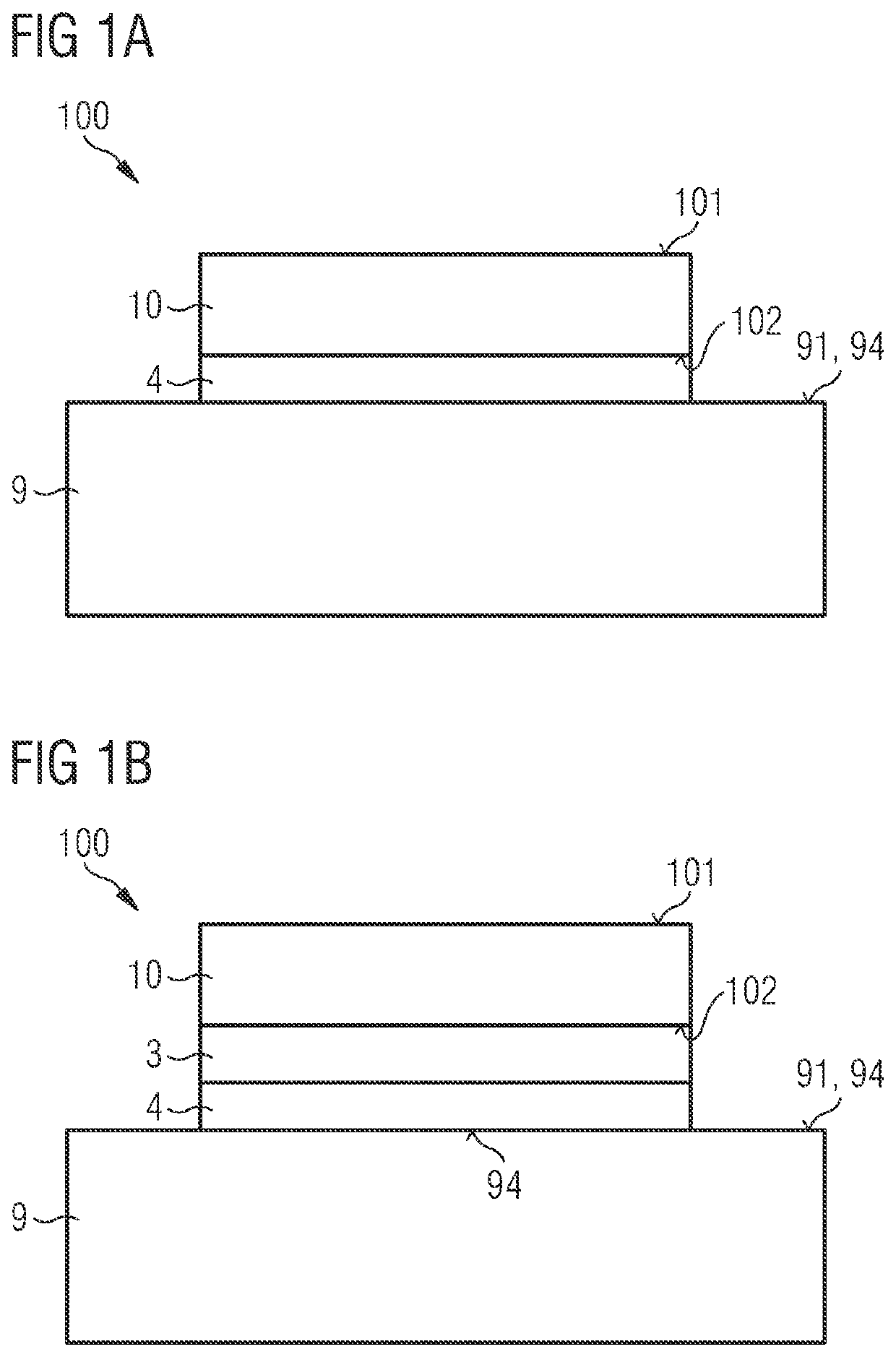
[0058]FIG. 1A shows a comparative example of a component 100 having a semiconductor chip 10 on a carrier 9, wherein the semiconductor chip 10 is attached to a first main surface 91 or to a mounting surface 94 of the carrier 9 by a connection layer 4.

[0059]The semiconductor chip 10 has a front side 101 and a rear side 102 facing away from the front side 101. A front side of component 100 may be formed by the front side 101 of the semiconductor chip 10. For example, the front side 101 is a radiation entrance surface or a radiation exit surface of the semiconductor chip 10 or of the component 100. In particular, the connection layer 4 adjoins both the mounting surface 94 of the carrier 9 and the rear side 102 of the semiconductor chip 10.

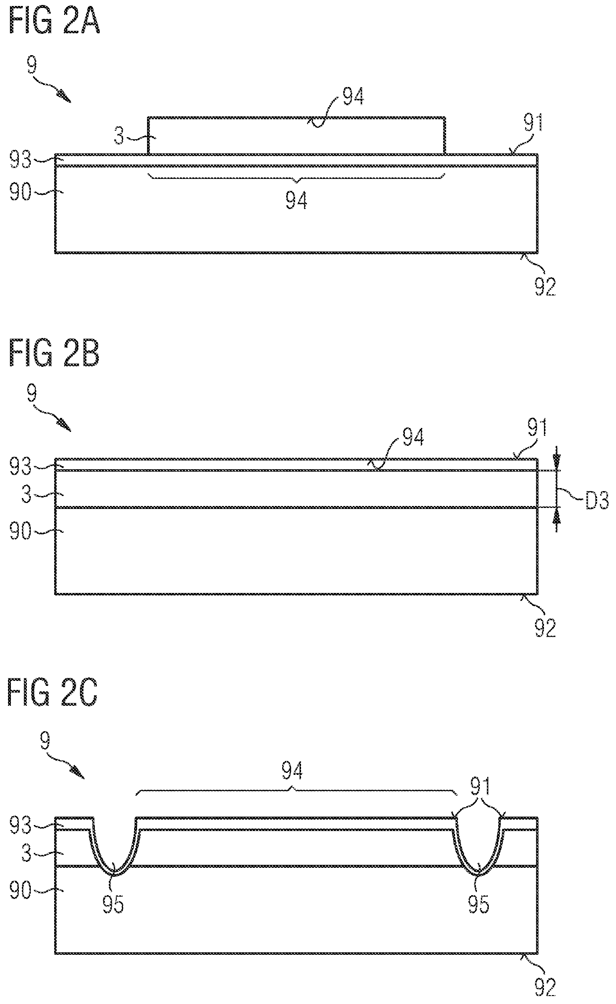
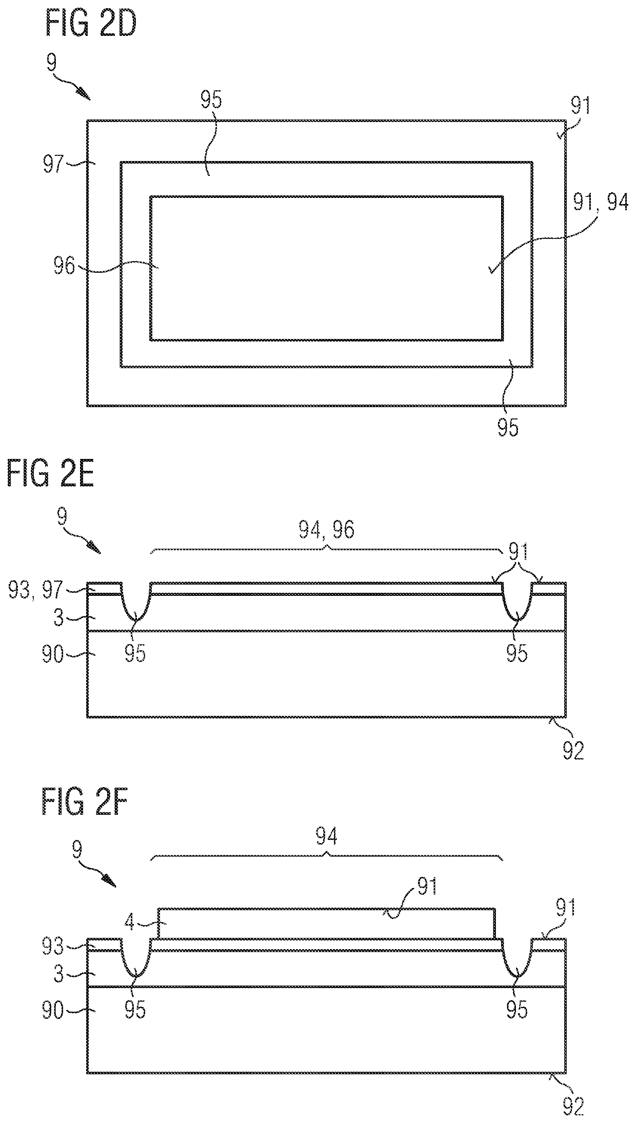
[0060]The semiconductor chip 10 comprising a substrate 1, a semiconductor body 2 and optionally a converter layer 6 is shown schematically in FIGS. 4A to 4C, for example.

[0061]In general, the carrier 9 and the semiconductor chip 10, especially the carr...


PUM

PropertyMeasurementUnit
yield stressaaaaaaaaaa
grain sizeaaaaaaaaaa

Abstract

A carrier and a component are disclosed. In an embodiment a component includes a semiconductor chip including a substrate and a semiconductor body arranged thereon and a metallic carrier having a coefficient of thermal expansion which is at least 1.5 times greater than a coefficient of thermal expansion of the substrate or of the semiconductor chip, wherein the semiconductor chip is attached to a mounting surface of the metallic carrier by a connection layer such that the connection layer is located between the semiconductor chip and a buffer layer and adjoins a rear side of the semiconductor chip, wherein the buffer layer has a yield stress which is at least 10 MPa and at most 300 MPa, and wherein the substrate of the semiconductor chip and the metallic carrier of the component have a higher yield stress than the buffer layer.

Description

[0001]This patent application is a national phase filing under section 371 of PCT / EP20 18 / 069910, filed Jul. 23, 2018, which claims the priority of German patent application 102017119344.8, filed Aug. 24, 2017, each of which is incorporated herein by reference in its entirety.TECHNICAL FIELD[0002]A carrier in particular for optoelectronic components is specified. In addition, a component, especially an optoelectronic component, having high mechanical stability is specified. Furthermore, a method for producing a component is specifiedBACKGROUND[0003]In the case of a component comprising a semiconductor chip which is attached to a metallic carrier by a connection layer, on the carrier side and on the semiconductor chip side internal thermo-mechanical tensions often occur in the event of temperature fluctuations due to different thermal expansion coefficients. The internal tensions can lead to damage, in particular to undesirable deformations of the component or of the semiconductor ch...

Claims


Application Information

Patent Timeline
Patent Type & Authority Applications(United States)
IPC IPC(8): H01L33/62H01L33/38H01L33/00
CPCH01L33/382H01L33/62H01L2933/0066H01L2933/0033H01L33/005H01L33/486
Inventor ALTIERI-WEIMAR, PAOLANEUDECKER, INGOZITZLSPERGER, MICHAELGROETSCH, STEFANKLASSEN, HOLGER
Owner OSRAM OLED
Why Eureka
Try Eureka