Image sensor employing avalanche diode
a technology of image sensor and avalanche diode, which is applied in the field of photon detection technology, can solve the problem that the spad cannot achieve the quenching by itself, and achieve the effect of low limitation on the minimum pixel size and high fill factor
- Summary
- Abstract
- Description
- Claims
- Application Information
AI Technical Summary
Benefits of technology
Problems solved by technology
Method used
Image
Examples
first embodiment
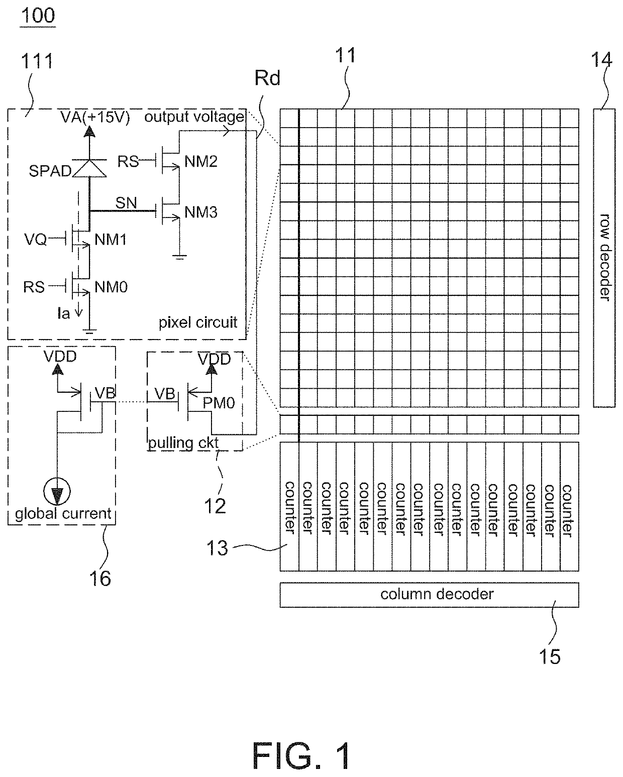
[0027]Referring to FIG. 1, it is a schematic diagram of an image sensor 100 according to the present disclosure. The image sensor 100 is used to detect extremely weak light and high frequency signals, and thus a single photon avalanche diode (SPAD) is employed to detect photon events. A processor generates an image frame by counting photon events of every pixel to perform the object tracking, gesture recognition, 3D image construction, and biological feature detection and recognition.
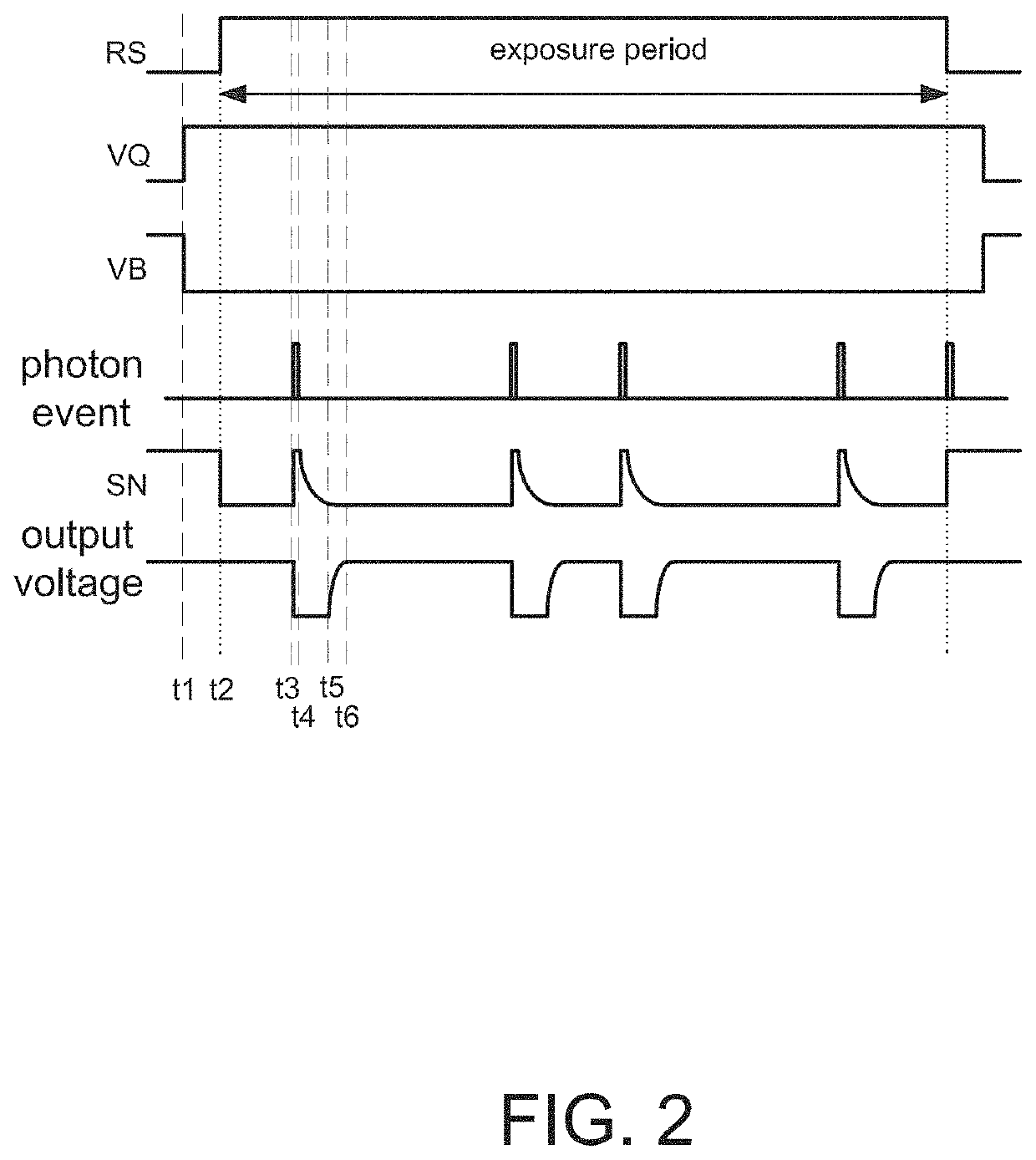
[0028]The image sensor 100 includes a pixel array 11, a plurality of pulling circuits 12, a plurality of counters 13, a row decoder 14, a column decoder 15 and a global current source circuit 16, wherein the row decoder 14 and the column decoder 15 are used to determine a pixel position in the pixel array 11 that is being exposed and outputting a detected signal (e.g., pulses mentioned below). The operation of the row decoder 14 and the column decoder 15 is known to the art and is not a main objective o...
second embodiment
[0046]Referring to FIG. 4, it is a schematic diagram of an image sensor 400 according to the present disclosure. The image sensor 400 is also used to detect extremely weak light and high frequency signals, and thus a single photon avalanche diode (SPAD) is employed to detect photon events. A processor generates an image frame by counting photon events of every pixel to perform the object tracking, gesture recognition, 3D image construction, and biological feature detection and recognition.
[0047]The image sensor 400 includes a pixel array 41, a plurality of pulling circuits 42, a plurality of counters 43, a row decoder 44, a column decoder 45 and a global current source circuit 46, wherein the row decoder 44 and the column decoder 45 are also used to determine a pixel position in the pixel array 41 that is being exposed and outputting a detected signal (e.g., pulses mentioned below).
[0048]The pixel array 41 includes a plurality of pixel circuits 411 (e.g., FIG. 4 also showing 16×16 p...
third embodiment
[0066]In the third embodiment, the image sensor 100 also includes a pixel array 11, a plurality of pulling circuits 12, a plurality of counters 13, a row decoder 14, a column decoder 15 and a global current source circuit 16. The pixel array 11 also includes a plurality of pixel circuits 111.
[0067]Each pixel circuit 111 includes an avalanche diode SPAD and at least a transistor NM3. A cathode of SPAD is connected to a positive bias voltage VA, e.g., +15V, but not limited to. An anode of SPAD is connected to a node SN that connects to a gate of the transistor NM3. Each of the plurality of pulling circuits 12 is configured to be coupled to a drain of the transistor NM3 of each pixel circuit 111 of one pixel circuit column via a readout line Rd.
[0068]Furthermore, to control the pixel circuit 111 in one pixel circuit column to detect a photo event sequentially, each pixel circuit 111 further includes another transistor NM2 connected between the transistor NM3 and the readout line Rd. Op...
PUM
| Property | Measurement | Unit |
|---|---|---|
| bias voltage | aaaaa | aaaaa |
| bias voltage | aaaaa | aaaaa |
| bias voltage | aaaaa | aaaaa |
Abstract
Description
Claims
Application Information


