Compact Optical Sensor For Fingerprint Detection

a fingerprint detection and optical sensor technology, applied in the field of compact optical sensors for fingerprint detection, can solve the problems of high cost, low yield, and substantial part of the desired light to be absorbed, and achieve the effect of cost-effective manufacturing and precise measuremen

Active Publication Date: 2020-09-10
WAVETOUCH LTD +1
View PDF12 Cites 17 Cited by
  • Summary
  • Abstract
  • Description
  • Claims
  • Application Information

AI Technical Summary

Benefits of technology

[0013]The present disclosure further relates to a method for fabrication of a microlens structure having aligned apertures that is suitable for use in the presently disclosed optical sensor system. The fabrication method is in a preferred embodiment directed to the use of a photosensitive material that is applied to the backside of the microlens structure. The photosensitive material may be any material which changes its properties upon receiving light, and by applying light, e.g. collimated light, through the front side of the microlens structure, the optical properties of the microlens structure can ensure that the precisely aligned transparent apertures are created in the photosensitive material on the backside of the microlens structure, thereby resulting in a precise but cost-efficient manufacturing of the microlens structure with transparent apertures in the backside.

Problems solved by technology

A problem with these absorbing channels is that a substantial part of the desired light is absorbed.
And the current technology used for manufacturing the absorbing channels is expensive and does not provide high yield.

Method used


Image

  • Compact Optical Sensor For Fingerprint Detection
  • Compact Optical Sensor For Fingerprint Detection
  • Compact Optical Sensor For Fingerprint Detection

Examples


examples

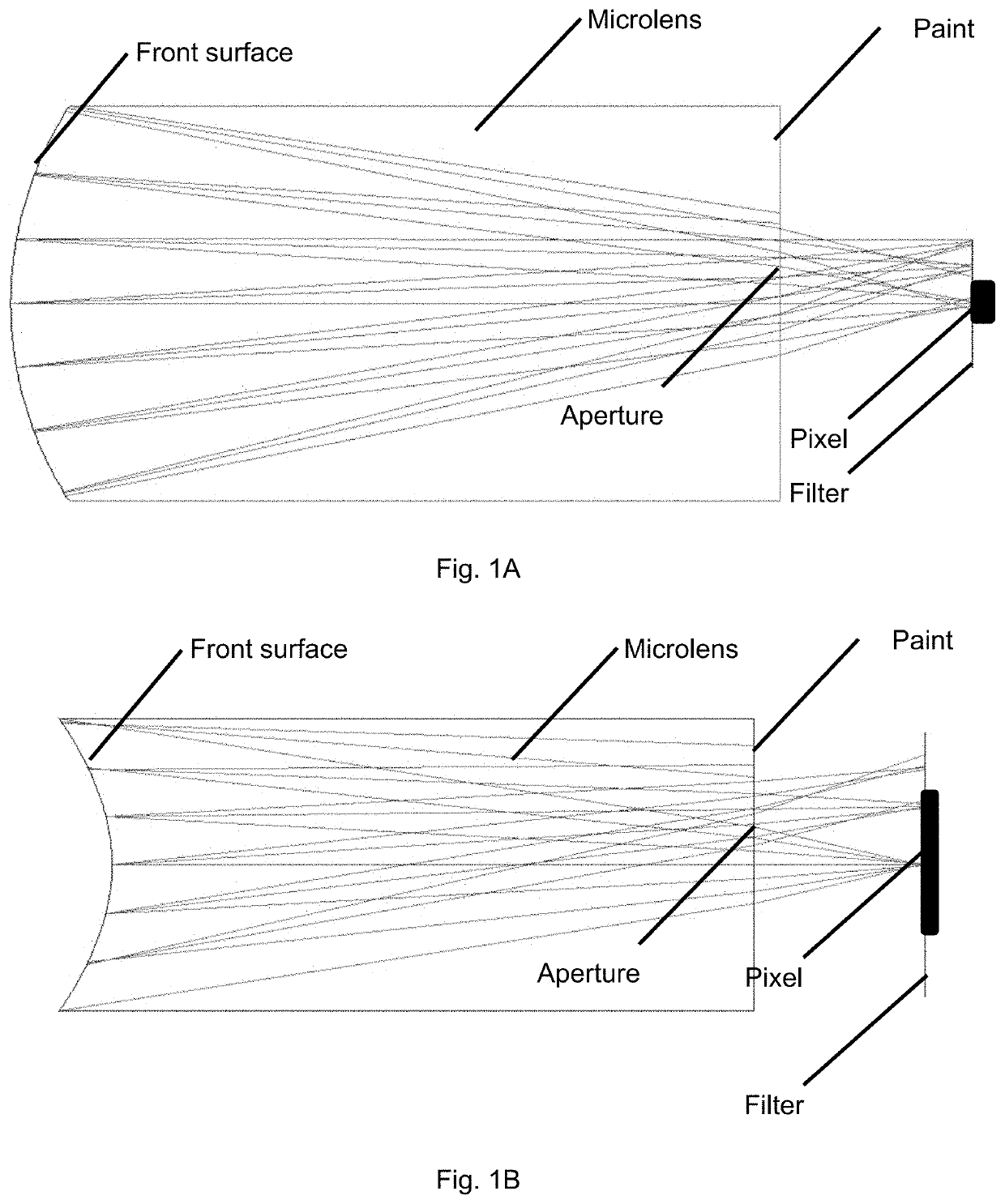
[0080]FIG. 1A shows a cut-through side view of an exemplary single microlens of a microlens structure as presently disclosed and a corresponding pixel. The focusing element at the front side of the microlens focuses light on to the pixel by means of a convex front surface. The convex front surface functions as focusing element when located in a medium with lower refraction index than itself, such as air. Part of the back side is painted to opaque. Unpainted part is the transparent aperture. Desired light pass through the aperture then hit the pixel which is an optical detector. Undesired light is absorbed by the paint, filtered by the filter, or hit outside of the pixel. The front side of the microlens in FIG. 1A is a sphere with radius of curvature of 24 microns, while the back side is a plane. The length of the microlens is 54 microns, width and height are both 24 microns. Back focal length is 13 microns. The transparent aperture in the center of the back side is circular and it f...


PUM

PropertyMeasurementUnit
incident angleaaaaaaaaaa
distanceaaaaaaaaaa

Abstract

The present disclosure relates to an optical sensor for use in an image recognition device, such as a fingerprint detector. The presently disclosed optical sensor has improved light transmittance in a compact and cost-efficient structure. In particular the presently disclosed optical sensor can be placed under a display panel of an electronic device, such as a smartphone. One embodiment relates to an optical sensor system for placement under a display panel for detecting/imaging light returned from a fingerprint on top of the display panel, the optical sensor comprising a microlens structure having a front side with an array of light focusing elements and an opaque back side with an array of optically transparent apertures aligned with the focusing elements, and a sensor array of optical detectors facing the back side of the microlens structure. The optical sensor system is preferably configured such that light returned from the object can be focused by the microlens structure onto the sensor array through the transparent apertures.

Description

RELATED APPLICATION(S)[0001]This application is a continuation of International Application No. PCT / EP2019 / 061738, which designated the United States and was filed on May 7, 2019, published in English, which claims priority to European Patent Application no. 18170996.5, filed May 7, 2018, and European Patent Application no. 18184693.2, filed Jul. 20, 2018. The entire teachings of the above application(s) are incorporated herein by reference.[0002]The present disclosure relates to an optical sensor for use in an image recognition device, e.g. a biometric recognition system, such as a fingerprint detector. The presently disclosed optical sensor has improved light transmittance in a compact and cost-efficient structure. In particular the presently disclosed optical sensor can be placed under a display panel of an electronic device, such as a smartphone.BACKGROUND OF INVENTION[0003]Fingerprint sensors have been massively integrated in electronic devices with displays, such as smartphone...

Claims


Application Information

Patent Timeline
Patent Type & Authority Applications(United States)
IPC IPC(8): G06F3/042G06K9/00
CPCG06K9/00053G06F3/0421G06K9/00046G06K9/0004G02B27/30G02B3/0056G06V40/1318G06F2203/0338G06V40/1324G06V40/1329
Inventor XIANG, PENGJENSEN, JØRGEN KORSGAARD
Owner WAVETOUCH LTD
Why Eureka
Try Eureka