Electronic component

Active Publication Date: 2020-10-01
TDK CORPARATION
View PDF0 Cites 5 Cited by
  • Summary
  • Abstract
  • Description
  • Claims
  • Application Information

AI Technical Summary

Benefits of technology

This patent describes a method for controlling the peeling off of a conductive resin layer from a surface. By designing the interface between the resin and the sintered metal layer, the gas generated from moisture absorbed by the resin can reliably pass through and reach the gap without causing stress on the resin layer. This results in a more efficient and reliable peeling off process.

Problems solved by technology

In this case, stress may act on the conductive resin layer, and the conductive resin layer may be cracked and be peeled off.

Method used


Image

  • Electronic component
  • Electronic component
  • Electronic component

Examples


Embodiment Construction

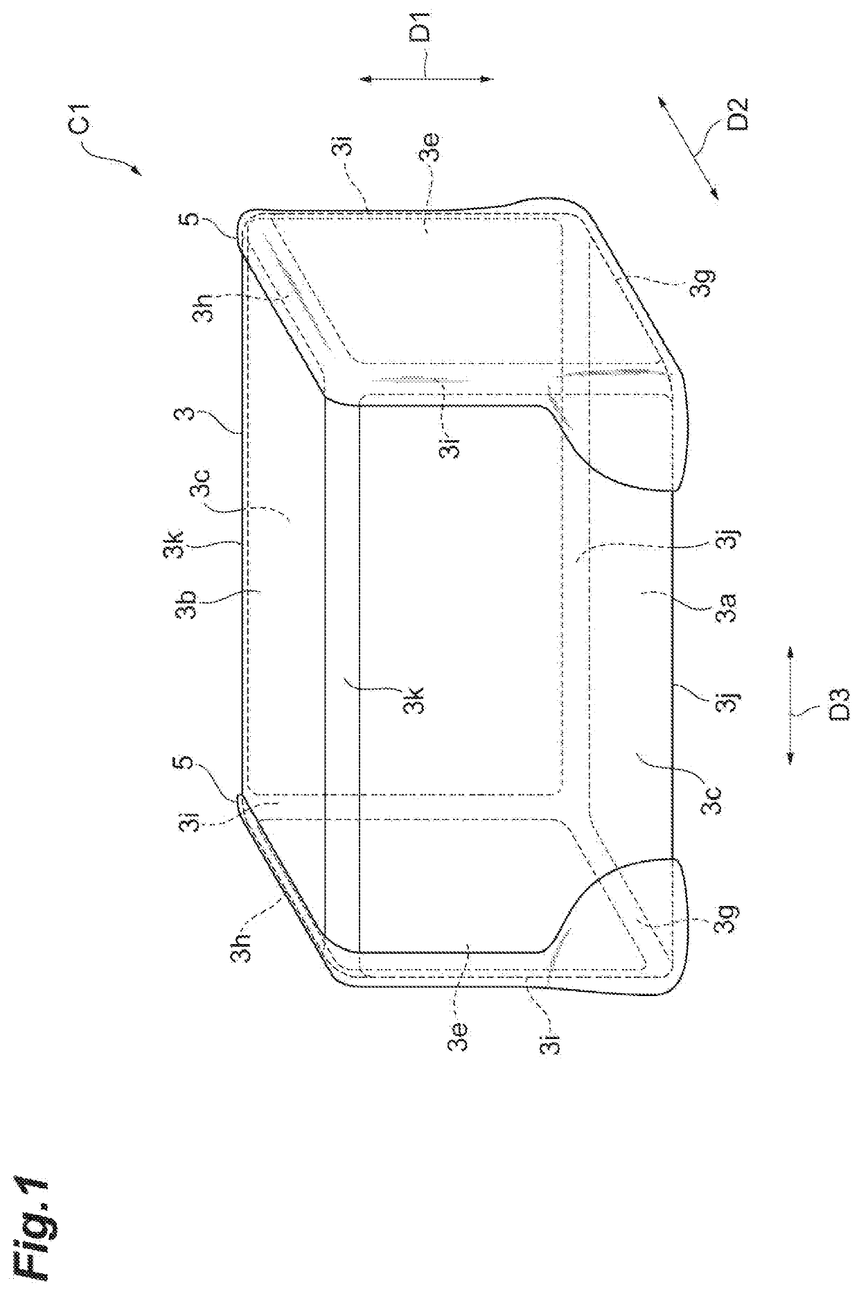
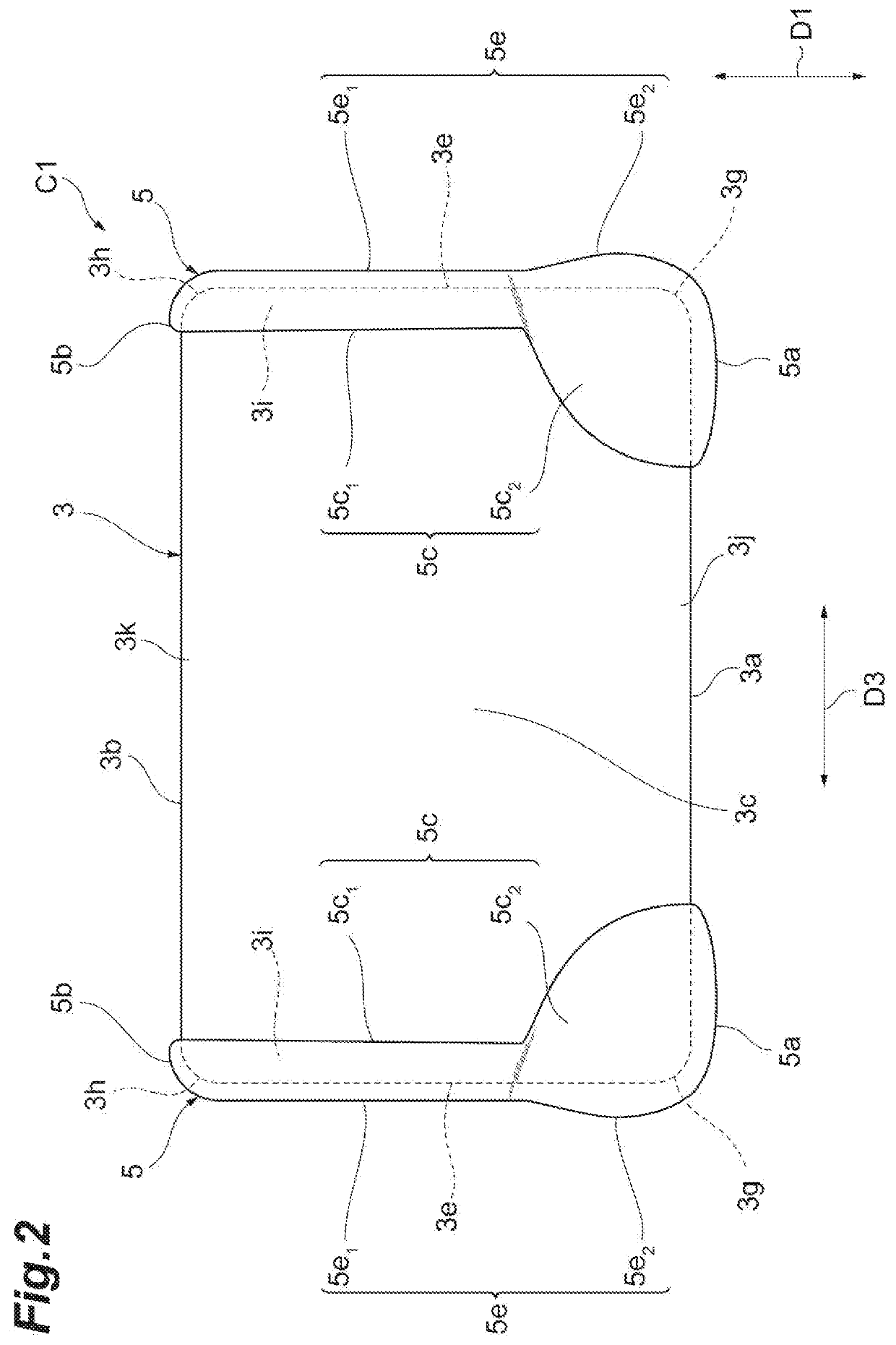
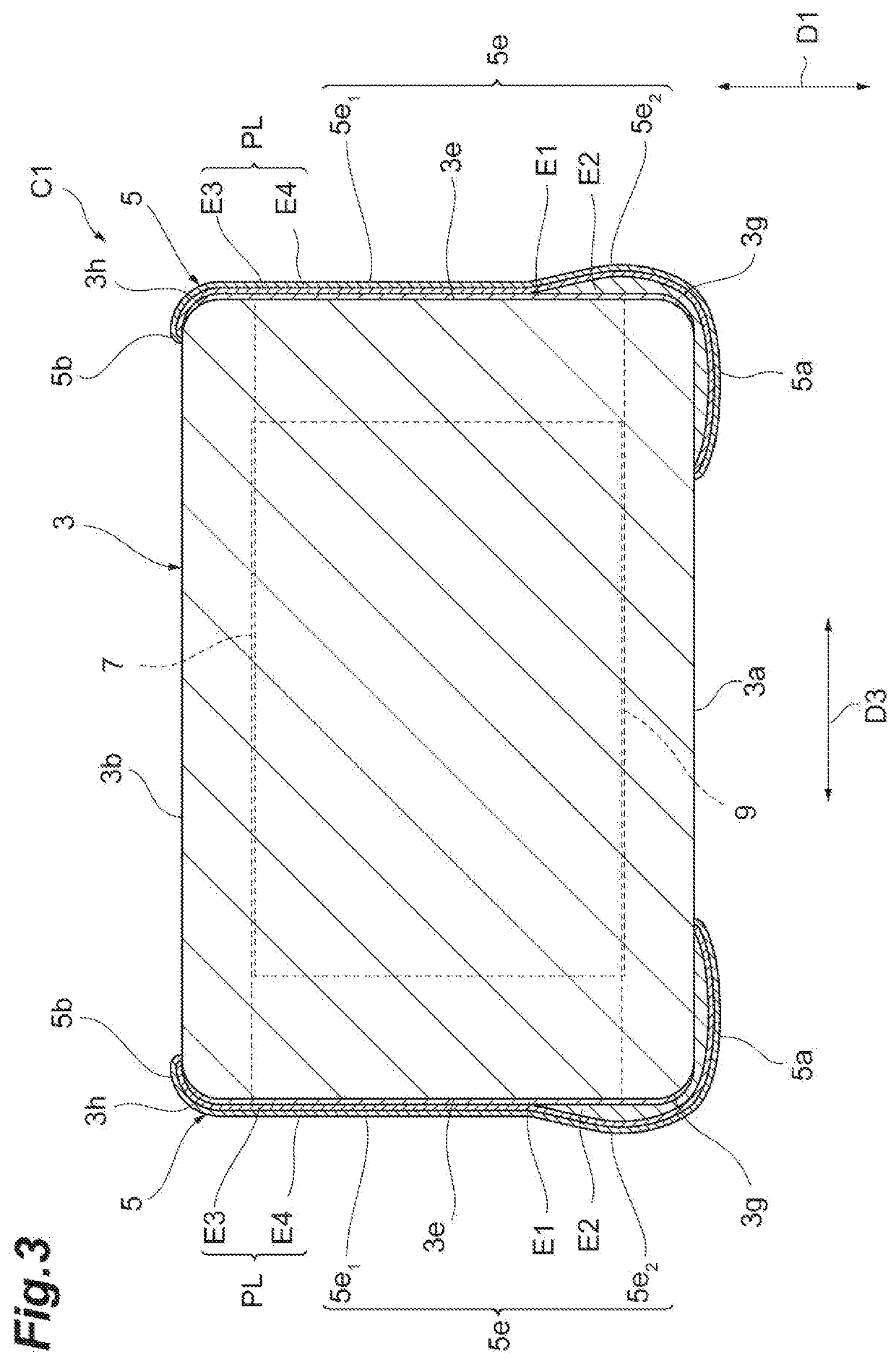
[0048]Hereinafter, embodiments of the present invention will be described in detail with reference to the accompanying drawings. In the following description, the same elements or elements having the same functions are denoted with the same reference numerals and overlapped explanation is omitted.

[0049]A configuration of a multilayer capacitor C1 according to an embodiment will be described with reference to FIGS. 1 to 9. FIG. 1 is a perspective view of a multilayer capacitor according to the embodiment. FIG. 2 is a side view of the multilayer capacitor according to the embodiment. FIGS. 3 to 5 are views illustrating a cross-sectional configuration of the multilayer capacitor according to the embodiment. FIG. 6 is a plan view illustrating an element body, a first electrode layer, and a second electrode layer. FIG. 7 is a side view illustrating the element body, the first electrode layer, and the second electrode layer. FIG. 8 is an end view illustrating the element body, the first e...


PUM


Abstract

An electronic component includes an element body and an external electrode. The element body includes a principal surface arranged to constitute a mounting surface and an end surface adjacent to the principal surface. The external electrode includes a conductive resin layer disposed to continuously cover a part of the principal surface and a part of the end surface, and a plating layer covering the conductive resin layer. The conductive resin layer includes a first region positioned on the end surface, a second region positioned on a ridge portion between the end surface and the principal surface, and a third region positioned on the principal surface. In a case where a maximum thickness of the first region is T1 (μm) and a minimum thickness of the second region is T2 (μm), the maximum thickness T1 and the minimum thickness T2 satisfy a relation ofT2 / T1≥0.26.

Description

BACKGROUND OF THE INVENTION1. Field of the Invention[0001]The present invention relates to an electronic component.2. Description of Related Art[0002]Known electronic components include an element body and an external electrode disposed on the element body (for example, refer to Japanese Unexamined Patent Publication No. 2018-157029). The element body includes a principal surface arranged to constitute a mounting surface and an end surface adjacent to the principal surface. The external electrode includes a conductive resin layer disposed to continuously cover a part of the principal surface and a part of the end surface, and a plating layer covering the conductive resin layer.SUMMARY OF THE INVENTION[0003]The conductive resin layer generally contains a resin and conductive particles. The resin tends to absorb moisture. In a case in which the electronic component is solder-mounted on an electronic device, the moisture absorbed by the resin may be gasified so that volume expansion ma...

Claims


Application Information

Patent Timeline
IPC IPC(8): H01G4/005H01G4/33
CPCH01G4/33H01G4/005H01G4/232H01G4/30H01G4/248
Inventor NAGAI, YUICHITAKEDA, ATSUSHITAMURA, TAKEHISAONODERA, SHINYA
Owner TDK CORPARATION
Why Eureka
Try Eureka