Wafer inspecting apparatus

a technology of wafers and inspection apparatuses, applied in the direction of image enhancement, semiconductor/solid-state device testing/measurement, instruments, etc., can solve the problem of large size of inspection apparatuses incorporating these cameras, and achieve the effect of easy determination of the image capture range of micro cameras

Active Publication Date: 2021-01-14
DISCO CORP
View PDF0 Cites 2 Cited by
  • Summary
  • Abstract
  • Description
  • Claims
  • Application Information

AI Technical Summary

Benefits of technology

[0007]According to the present invention, even in the case where the center coordinates of the holding surface and the center coordinates of the wafer are displaced out of alignment with each other, allowing the position in the X-axis directions of the outer circumference of the wafer to vary as the holding table rotates, the control unit can make the image capturing range of the micro camera follow the varying position of the outer circumference of the wafer. Therefore, the image capturing range of the micro camera can be determined with ease even if the center coordinates of the holding surface and the center coordinates of the wafer are displaced out of alignment with each other.
[0008]Furthermore, images of both the surface of the wafer and the outer circumference of the wafer can be captured and both the surface of the wafer and the outer circumference of the wafer can be inspected simply when the macro camera and the micro camera are moved along the X-axis directions by the single X-axis moving mechanism. The wafer inspecting apparatus can thus easily be rendered compact.

Problems solved by technology

If the cameras are combined with respective moving means for moving the cameras to the respective areas whose images are to be captured by the cameras, then an inspecting apparatus incorporating these cameras tends to large in size.

Method used


Image

  • Wafer inspecting apparatus
  • Wafer inspecting apparatus
  • Wafer inspecting apparatus

Examples


Embodiment Construction

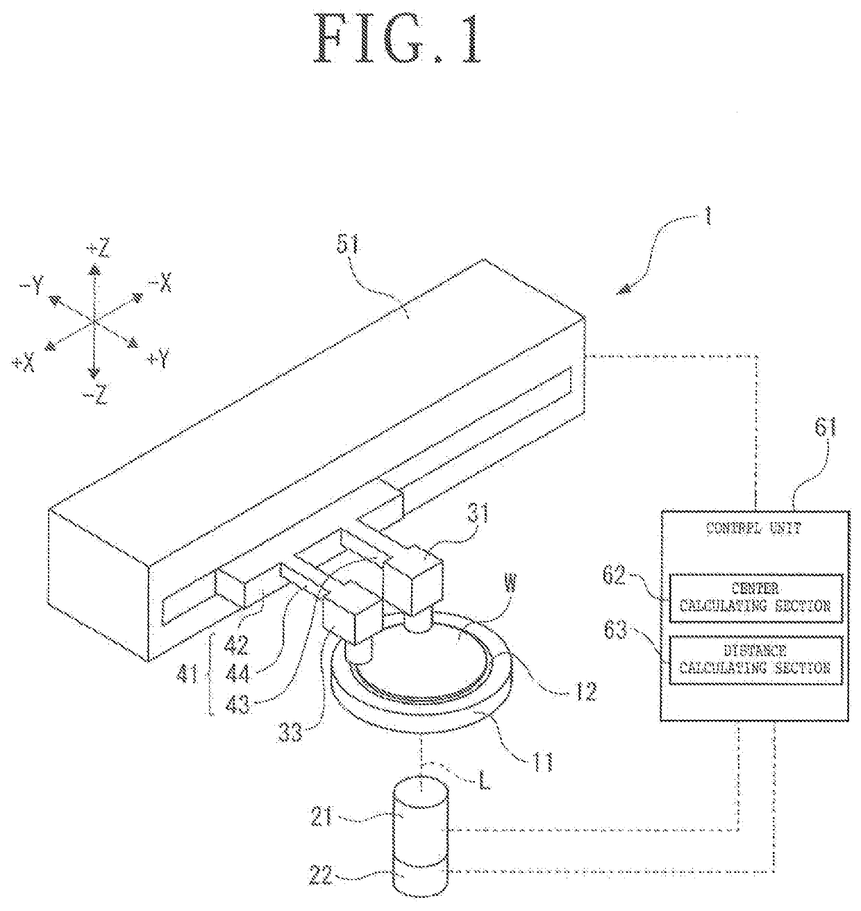
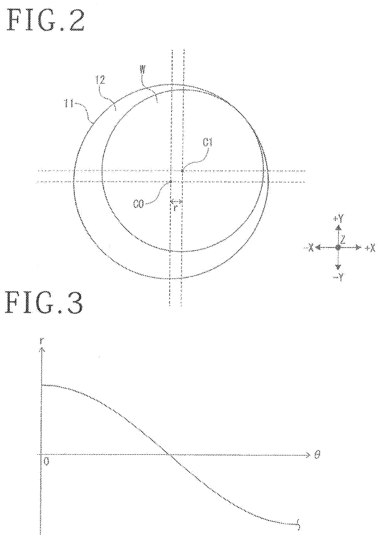
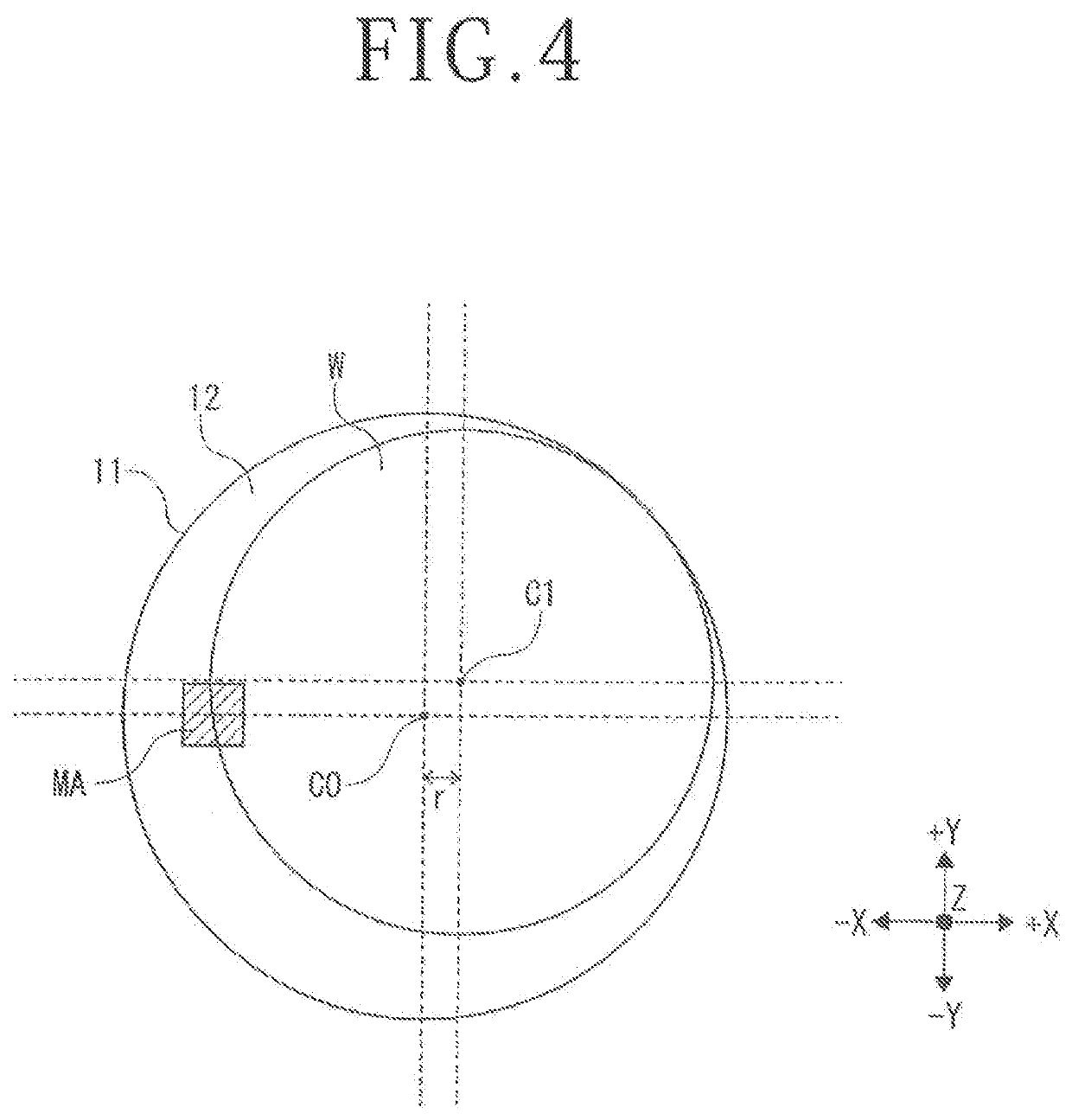
[0014]A wafer inspecting apparatus 1 according to a preferred embodiment of the present invention illustrated in FIG. 1 is an apparatus for capturing images of a surface and an outer circumference of a wafer W and inspecting the surface and the outer circumference of the wafer W on the basis of the captured images. Particularly, the wafer inspecting apparatus 1 captures images of a ground surface and an outer circumference of the wafer W and inspecting the ground surface and the outer circumference of the wafer W on the basis of the captured images.

[0015]As illustrated in FIG. 1, the wafer inspecting apparatus 1 includes a holding table 11 for holding the wafer W thereon, an electric motor 21 for rotating the holding table 11, and an encoder 22. The holding table 11 has a holding surface 12 for holding the wafer W thereon. The holding surface 12 includes, for example, a porous ceramic material and is selectively held in fluid communication with a suction source, not illustrated, for...


PUM

PropertyMeasurementUnit
sizeaaaaaaaaaa
sizeaaaaaaaaaa
circumferenceaaaaaaaaaa

Abstract

A micro camera is placed in an appropriate image capturing position therefor on the basis of a center-to-center distance depending on a rotational angle of a holding table. Even in the case where the center C0 of a holding surface and the center C1 of a wafer are displaced out of alignment with each other, allowing a position in X-axis directions of an outer circumference of the wafer to vary as the holding table rotates, a control unit can make an image capturing range of the micro camera follow the varying position of the outer circumference of the wafer. Therefore, the image capturing range of the micro camera can be determined with ease. Both a surface of the wafer and the outer circumference of the wafer can be inspected simply when two cameras are moved along the X-axis directions by a single X-axis moving mechanism.

Description

BACKGROUND OF THE INVENTIONField of the Invention[0001]The present invention relates to a wafer inspecting apparatus.Description of the Related Art[0002]It has been customary in the art to capture an image of a surface of a wafer that has been ground by grinding stones and inspect the state of the ground surface of the wafer on the basis of the captured image (see JP 2016-049581A and JP 2016-075554A). There is also a technology for capturing an image of the edge of a wafer with an image capturing unit and inspecting the edge of the wafer to ascertain whether or not the edge has chipped on the basis of the captured image.[0003]For inspecting the ground surface of a wafer, an image capturing camera having a wide field of vision, i.e., a wide image capturing range, or a macro camera, is used in order to shorten the time required to inspect the ground surface. For inspecting the edge of a wafer, on the other hand, an image capturing camera having a narrow field of vision, i.e., a narrow...

Claims


Application Information

Patent Timeline
Patent Type & Authority Applications(United States)
IPC IPC(8): G06T7/00G01N21/95H01L21/687H01L21/66
CPCG06T7/0004G01N21/9501G06T2207/30148H01L22/12H01L21/68714G01N21/8851G01N21/01G01N21/84G01N2021/887G01N2021/0112G01N2021/8477G01N21/9503G01N21/8806G01N2021/8809G01N2021/0367
Inventor YOSHIDA, SHINJIHASHIMOTO, KOJINOMURA, YASUKUNI
Owner DISCO CORP
Why Eureka
Try Eureka