
Semiconductor package and camera module

a technology of semiconductors and camera modules, applied in semiconductor devices, television systems, radio control devices, etc., can solve problems such as the decrease of mounting stability, and achieve the effect of reducing size and ensuring mounting stability

Active Publication Date: 2021-01-21
ASAHI KASEI ELECTRONICS CO LTD
View PDF0 Cites 0 Cited by
  • Summary
  • Abstract
  • Description
  • Claims
  • Application Information

AI Technical Summary

Benefits of technology

This configuration enables the reduction of the camera module's size without affecting stability, allowing for increased lens aperture without enlarging the camera module, thus enhancing camera performance and reducing terminal thickness.

Problems solved by technology

When the size of the terminals t is reduced, there arises a problem that the stability in mounting decreases.

Method used


Image

  • Semiconductor package and camera module
  • Semiconductor package and camera module
  • Semiconductor package and camera module

Examples


Embodiment Construction

[0022]In the following detailed description, a large number of particular specific configurations are described to provide a perfect understanding of an embodiment of the present invention. However, it is clear that the other embodiments can be implemented without being limited to such particular specific configurations. Moreover, the following embodiment does not limit the present invention according to Claims and includes all the combinations of characteristic configurations described in the embodiment.

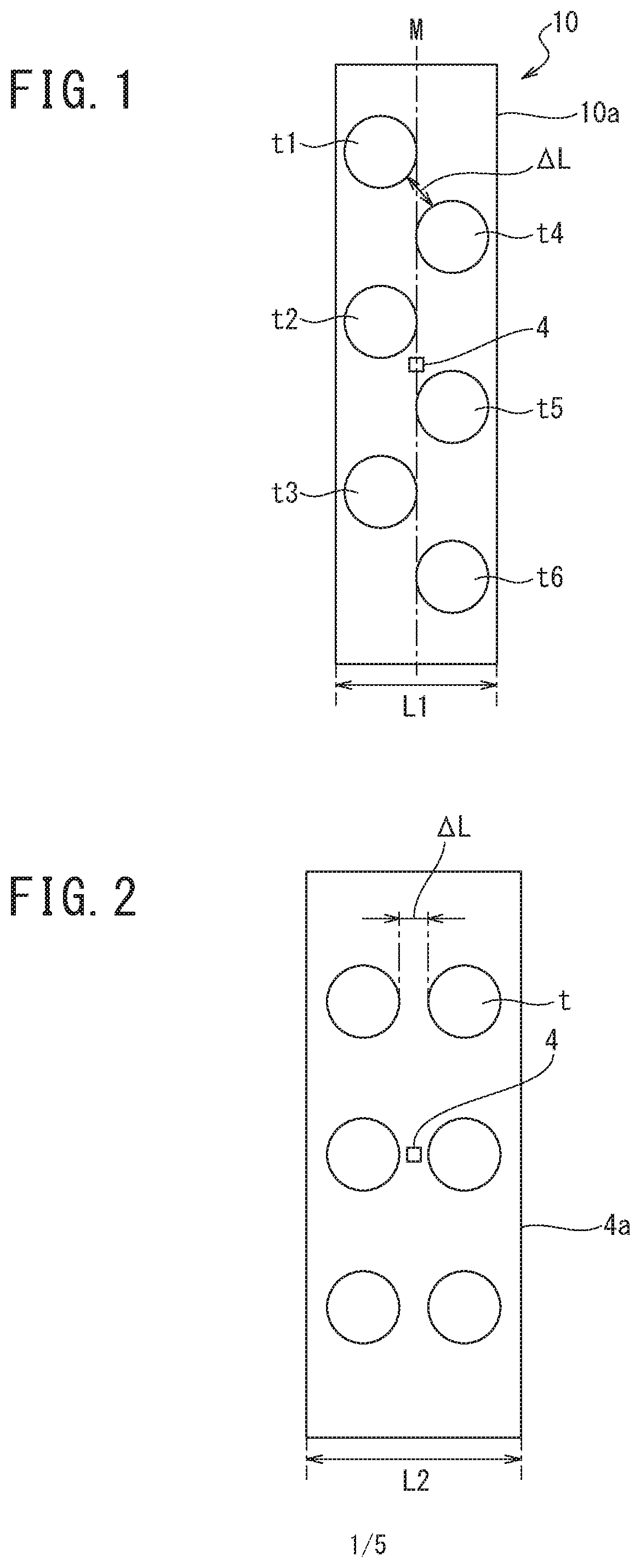
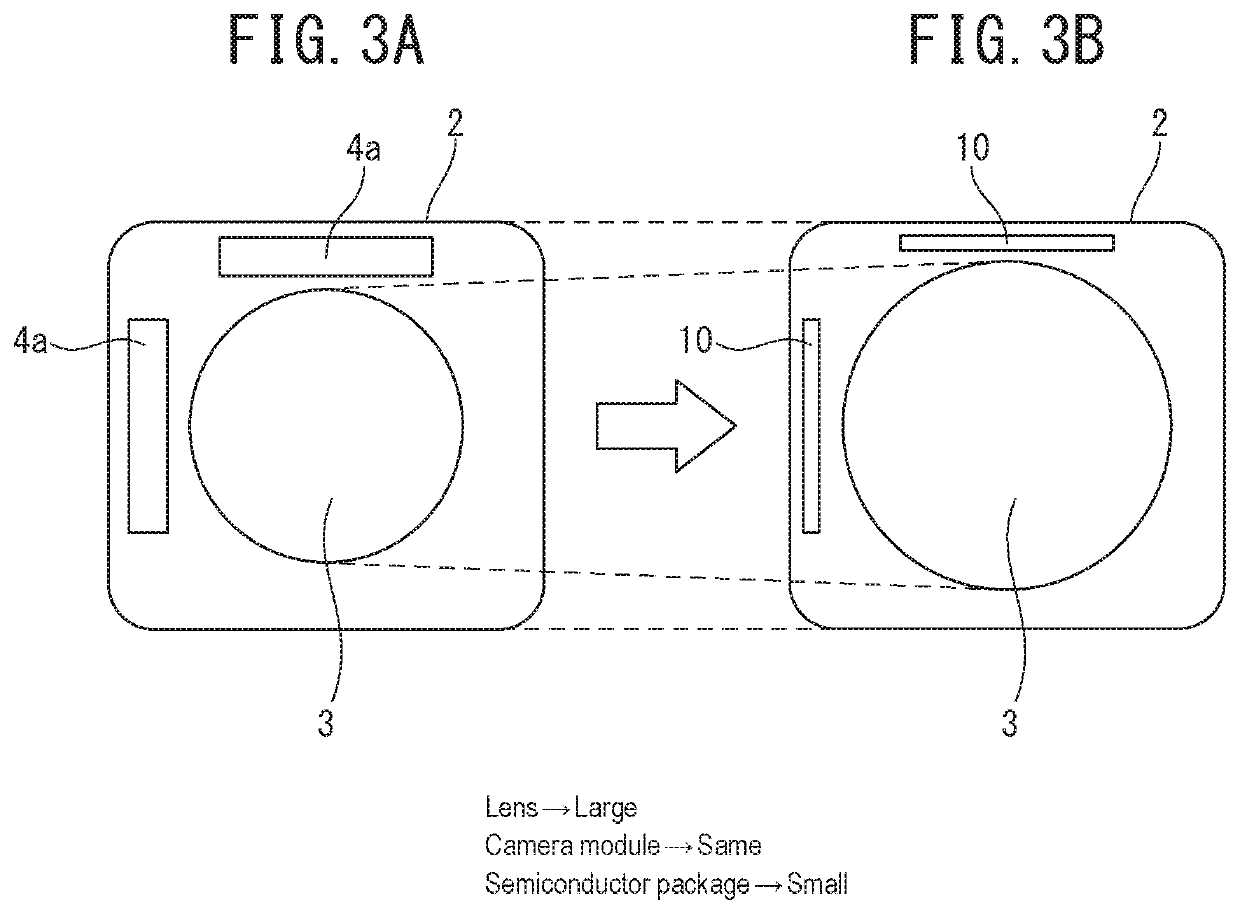
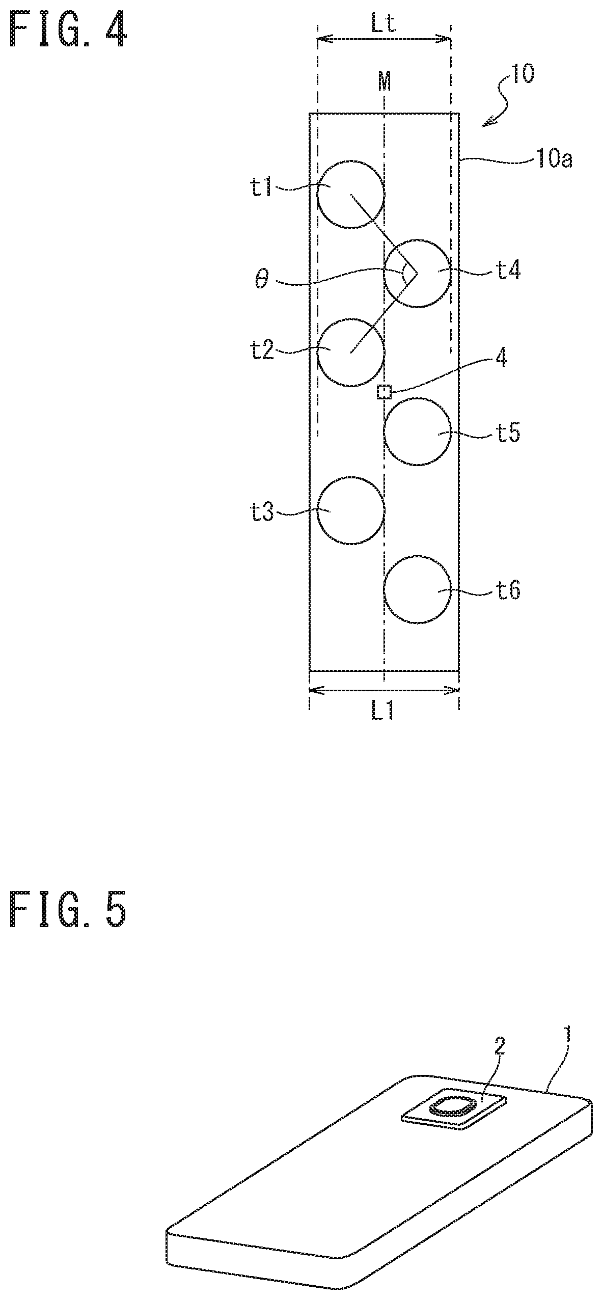
[0023]Hereinafter, one embodiment of the present invention is described with reference to the drawings. In the following description of the drawings, the same portions are designated by the same reference numerals. The drawings are schematically illustrated and the relationship between the thickness and the plane dimension, the ratio of the thickness of each layer, and the like are different from the actual relationship, ratio, and the like.

[0024]The embodiment of the present invent...


PUM


Abstract

To achieve a size reduction of a semiconductor package while securing stability in mounting.Three terminals t1, t2, and t4 are individually arranged on a semiconductor package 10 having a rectangular shape as viewed in plan in such a manner that the center in the longitudinal direction of the semiconductor package 10 of each of the three terminals t1, t2, and t4 and the center in the longitudinal direction of each of the other terminals are not overlapped with each other as viewed from the side of the long side. The terminal t4 and the other terminals t1 and t2 are arranged in such a manner that the terminal t4 and the other terminals t1 and t2 are present on mutually different sides across a line segment M passing through the center in the width direction, an angle θ formed by two line segments connecting the center of gravity of the terminal t4, the position in the longitudinal direction of which is the center, and the center of gravity of each of the other terminals t1 and t2 is 60° or more, and a width L1 of the semiconductor package 10 and a distance Lt between the rightmost end position of the terminal t4 arranged at the rightmost end in the width direction of the semiconductor package 10 and the leftmost end position of the terminal t1 or t2 arranged at the leftmost position in the width direction satisfy Lt / L1≥0.5.

Description

RELATED APPLICATION DATA[0001]This application is a continuation of and claims the benefit of priority to U.S. application Ser. No. 16 / 202,665, filed Nov. 28, 2018, which claims the benefit of priority to Japanese Application No. 2018-200361, filed Oct. 24, 2018, and to Japanese Application No. 2017-227584, filed Nov. 28, 2017; the entire contents of each of these applications are incorporated herein by reference.BACKGROUND OF THE INVENTIONField of the Invention[0002]The present invention relates to a semiconductor package and a camera module including the semiconductor package.Description of the Related Art[0003]In recent years, a camera module 2 is mounted in a mobile terminal 1, such as a smartphone or a cellular phone. The camera module2 has a lens 3 of a camera, semiconductor packages 4a each mounted with a sensor 4 for position detection of the lens 3 and the like, and a lens control mechanism including a coil 5, a magnet 6, or the like for adjusting the position of the lens 3...

Claims


Application Information

Patent Timeline
Patent Type & Authority Applications(United States)
IPC IPC(8): H01L27/146
CPCH01L27/14636H04N5/2253H01L27/14627H01L27/14618H04N23/54
Inventor SHIRATA, OSAMUHIDAKA, YUSUKE
Owner ASAHI KASEI ELECTRONICS CO LTD
Features
  • Generate Ideas
  • Intellectual Property
  • Life Sciences
  • Materials
  • Tech Scout
  • Unparalleled Data Quality
  • Higher Quality Content
  • 60% Fewer Hallucinations
Learn More