Processing method and resin applying machine

Active Publication Date: 2021-01-28
DISCO CORP
View PDF0 Cites 0 Cited by
  • Summary
  • Abstract
  • Description
  • Claims
  • Application Information

AI Technical Summary

Benefits of technology

The present invention aims to improve the consistency of coating thickness by providing a method for processing and applying resin to wafers. This results in a reduction in variations in the thickness of the resin, which enhances the overall quality of the coated wafers.

Problems solved by technology

Furthermore, since a predetermined fixed value is given to indicate how close the holder and the table should be to each other in coating the wafer with the resin, any thickness variations of the wafer are liable to fail to coat the wafer to a uniform thickness with the resin.

Method used


Image

  • Processing method and resin applying machine
  • Processing method and resin applying machine
  • Processing method and resin applying machine

Examples


first embodiment

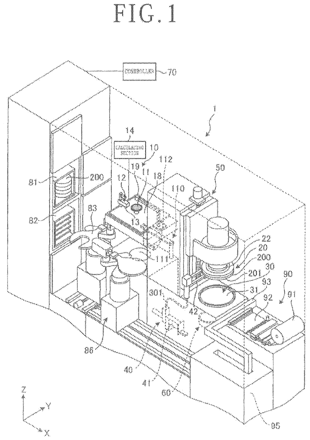
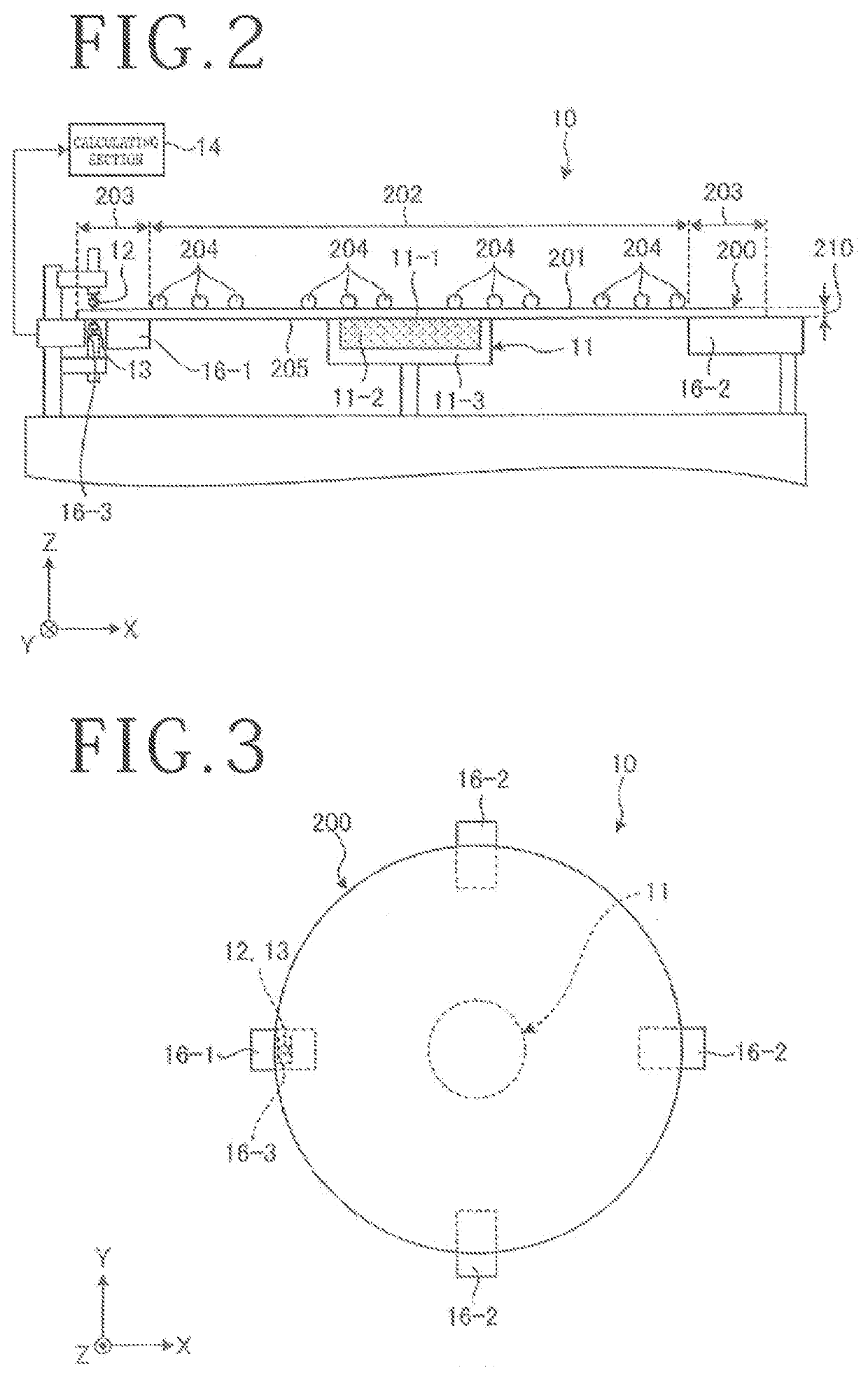
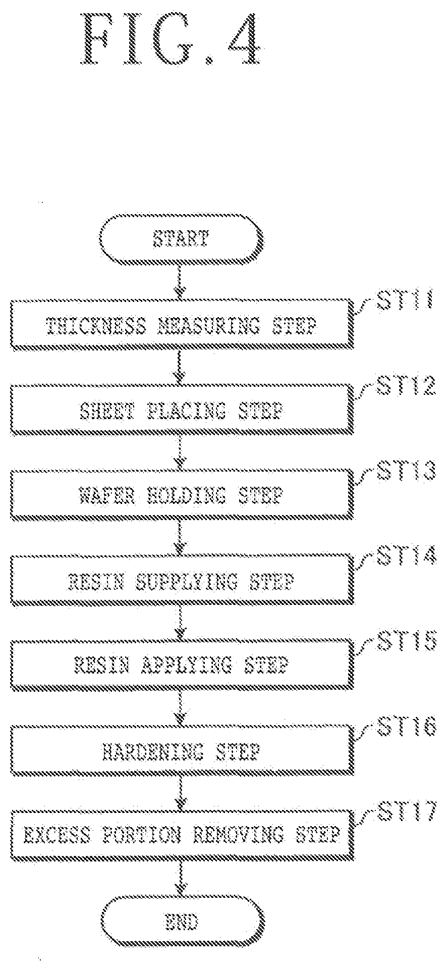
[0024]A resin applying machine 1 and a processing method according to a first embodiment of the present invention will be described below with reference to the drawings. FIG. 1 illustrates in perspective a structural example of the resin applying machine 1 according to the first embodiment. FIG. 2 illustrates in cross section essential details of a thickness measuring unit 10 of the resin applying machine 1 illustrated in FIG. 1. FIG. 3 illustrates in plan the essential details of the thickness measuring unit 10 of the resin applying machine 1 illustrated in FIG. 1. The resin applying machine 1 is an apparatus that carries out a processing method for coating a face side 201 that is one surface of a wafer 200 with a resin 302.

[0025]According to the first embodiment, the wafer 200, which is an object to be coated with the resin 302 by the resin applying machine 1, is a semiconductor wafer, an optical device wafer, or the like that is shaped as a circular plate made of a base material ...

second embodiment

[0075]A resin applying machine 1 and a processing method according to a second embodiment of the present invention will be described below with reference to the drawings. FIGS. 12A and 12B illustrate in cross section essential details of a tape affixing step according to the second embodiment. FIG. 12A illustrates the wafer 200 and a tape 220 before the tape 220 is affixed to the wafer 200. FIG. 12B illustrates the wafer 200 and the tape 220 after the tape 220 has been affixed to the wafer 200. FIG. 13 illustrates in cross section essential details of resin applying step ST15 according to the second embodiment. Those parts in FIGS. 12A, 12B, and 13 which are identical to those of the first embodiment are denoted by identical reference characters, and will not be described in detail below.

[0076]The resin applying machine 1 according to the second embodiment is similar to the resin applying machine 1 according to the first embodiment except that a tape affixing unit 120 is added. As i...


PUM


Abstract

There is provided a processing method including the steps of measuring a thickness of the wafer, holding the wafer on a holder, supplying a liquid resin to a table that faces the holder, relatively moving the holder and the table closely to each other to coat the wafer with the liquid resin, and hardening the liquid resin that has coated the wafer. In the resin applying step, a distance by which the holder and the table are to be relatively moved closely to each other to coat the wafer with the liquid resin is determined depending on the measured thickness of the wafer.

Description

BACKGROUND OF THE INVENTIONField of the Invention[0001]The present invention relates to a processing method and a resin applying machine for coating one surface of a wafer with a resin.Description of the Related Art[0002]There is known a technology in which a holder holding a wafer and a table supplied with a liquid resin are brought closely to each other to coat one surface of the wafer with the resin (see Japanese Patent Laid-Open No. 2016-167546).SUMMARY OF THE INVENTION[0003]In a case where a bumpy surface of a wafer with bumps is coated with a resin to make the surface irregularities even and the opposite surface of the wafer is cut or ground, if the resin layer is not of a constant thickness, the wafer tends to be cut to varying depths or ground to different thicknesses. Furthermore, since a predetermined fixed value is given to indicate how close the holder and the table should be to each other in coating the wafer with the resin, any thickness variations of the wafer are lia...

Claims


Application Information

Patent Timeline
IPC IPC(8): H01L21/67H01L21/56
CPCH01L21/6715H01L21/67253H01L21/56H01L21/67132H01L22/12H01L22/20H01L21/561H01L21/67115H01L21/67092H01L21/6835H01L2221/6834
Inventor MIGIYAMA, YOSHIKUNISUGIURA, KAZUKIKAKINUMA, YOSHINORIIKUSHIMA, MITSURU
Owner DISCO CORP
Why Eureka
Try Eureka