Method for decreasing sheet resistivity variations of an interconnect metal layer

Active Publication Date: 2008-04-15
ADVANCED MICRO DEVICES INC
View PDF6 Cites 0 Cited by
  • Summary
  • Abstract
  • Description
  • Claims
  • Application Information

AI Technical Summary

Benefits of technology

[0007]According to this embodiment, the method further includes performing a planarizing process to form a number of interconnect lines, where each of the interconnect lines is situated in one of the trenches. The planarizing process can be a chemical mechanical polishing process, for example. The dome-shaped profile of the metal layer causes the dielectric layer to have a substantially planar top surface after performing the planarizing process and causes the interconnect lines to have a reduced thickness variation across the wafer. The interconnect lines are situated in an interconnect metal layer, where the dome-shaped profile of the metal layer causes the interconnect metal layer to have increased sheet resistivity uniformity across the wafer after performing the planarizing process. Other features and advantages of the present invention will become more readily apparent to those of ordinary skill in the art after reviewing the following detailed description and accompanying drawings.

Problems solved by technology

Variations in sheet resistivity of an interconnect metal layer, such as a first interconnect metal layer (i.e. “M1”) of a semiconductor wafer, can undesirably reduce the manufacturing yield of semiconductor devices, such as memory and logic devices.
As a result, the thickness of the interconnect lines can vary significantly across the wafer, which can cause undesirable variations in sheet resistivity of the interconnect metal layer.

Method used


Image

  • Method for decreasing sheet resistivity variations of an interconnect metal layer
  • Method for decreasing sheet resistivity variations of an interconnect metal layer
  • Method for decreasing sheet resistivity variations of an interconnect metal layer

Examples


Embodiment Construction

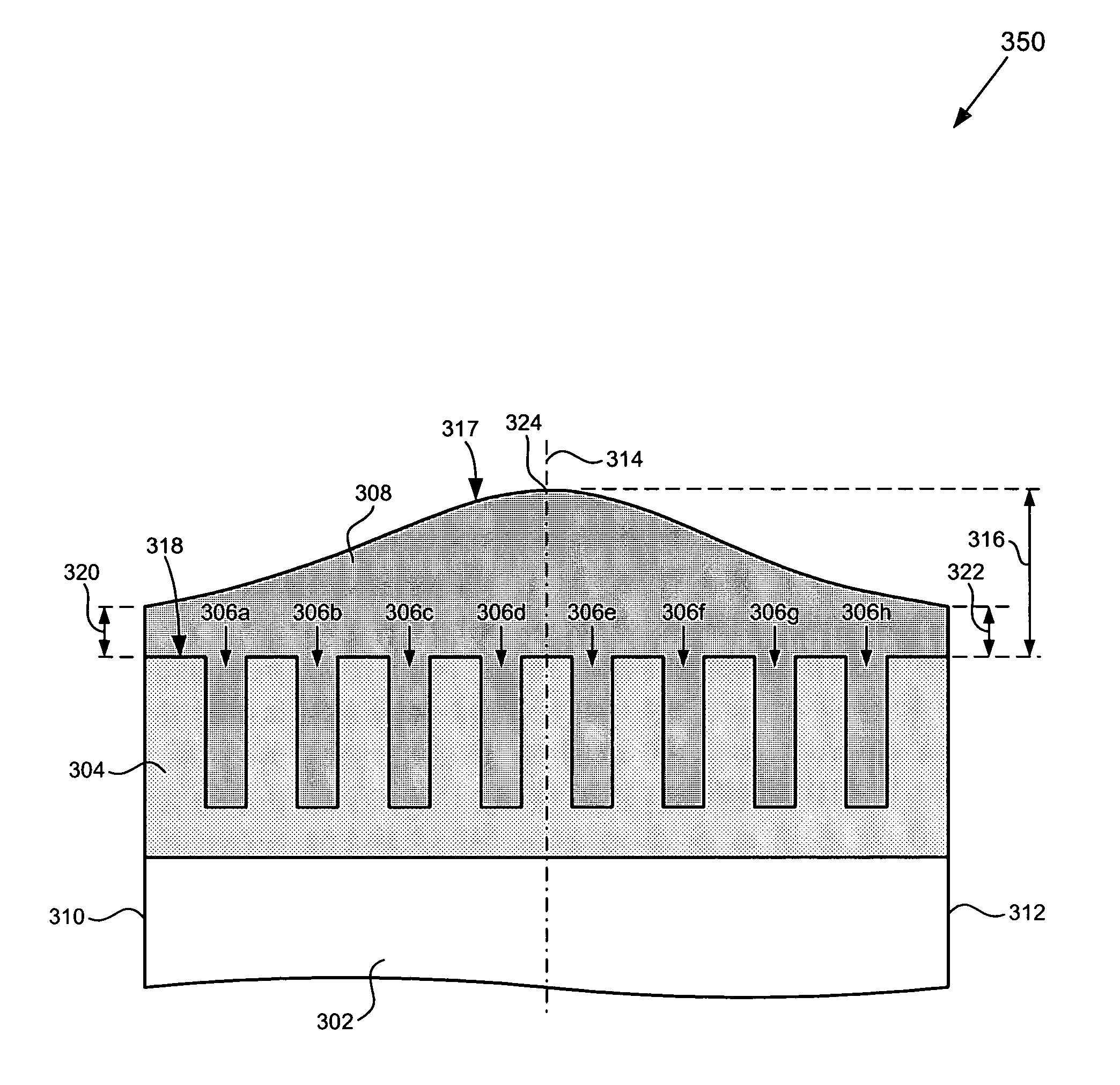
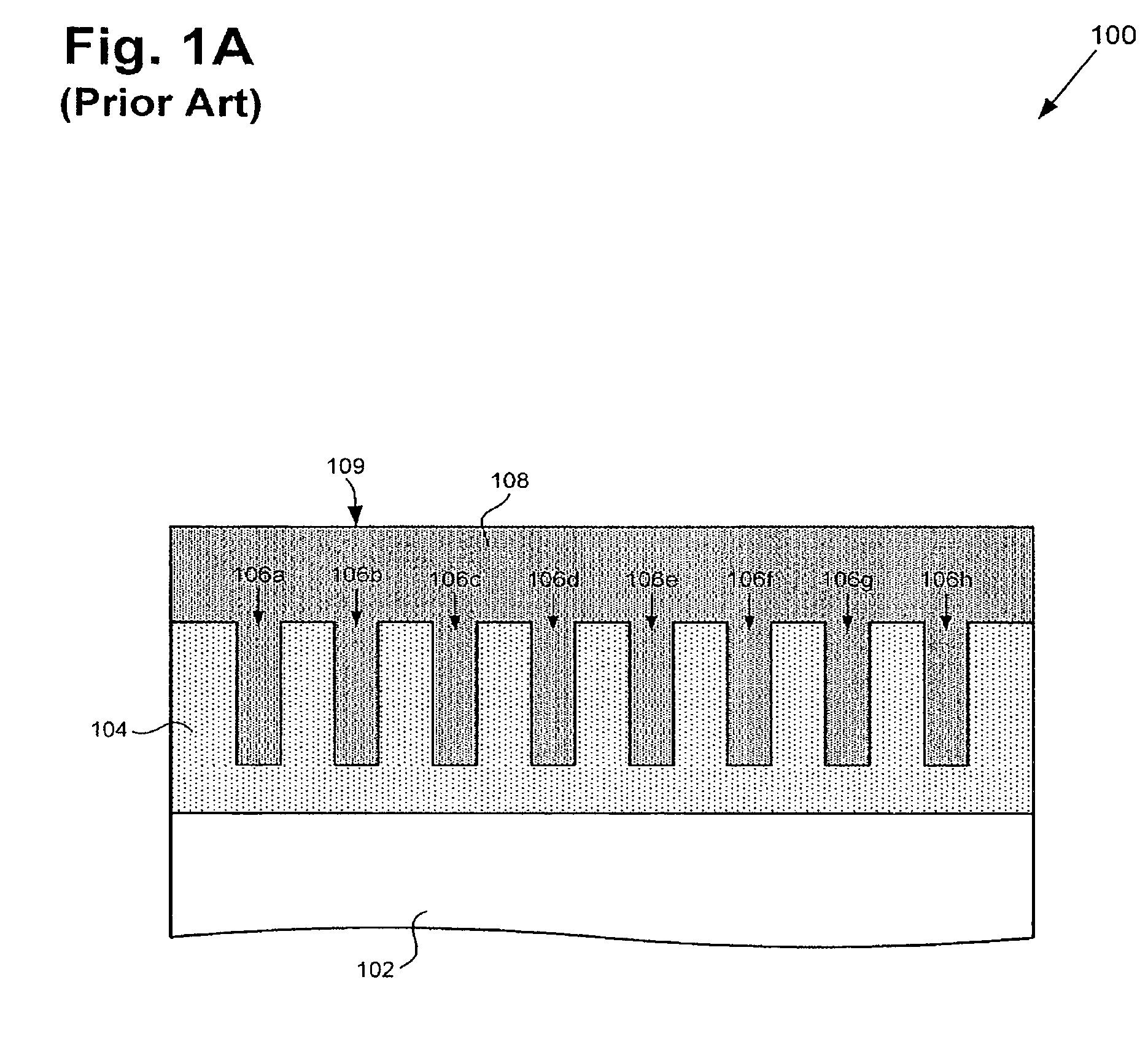
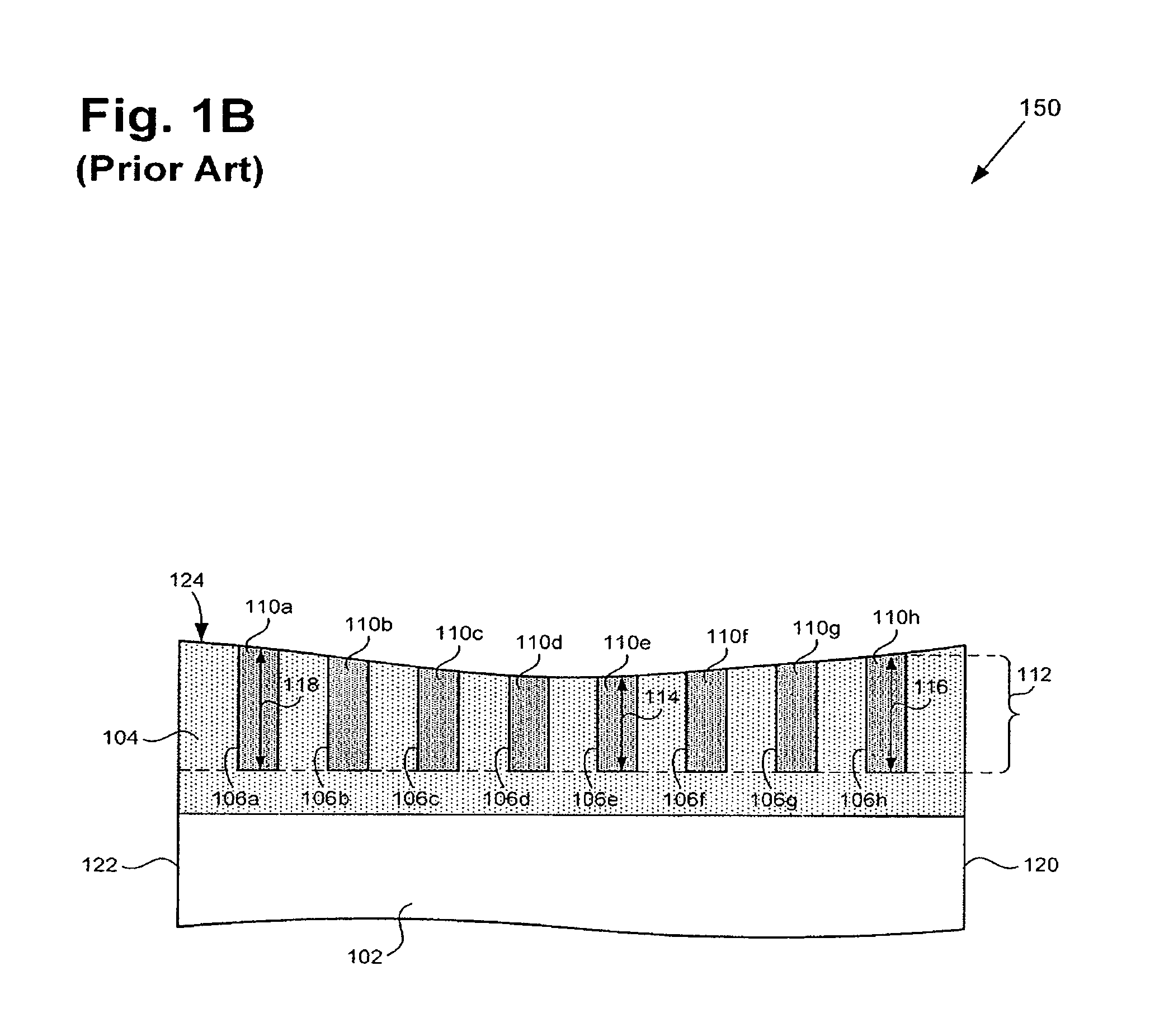
[0016]The present invention is directed to a method for reducing variations in sheet resistivity of an interconnect metal layer. The following description contains specific information pertaining to the implementation of the present invention. One skilled in the art will recognize that the present invention may be implemented in a manner different from that specifically discussed in the present application. Moreover, some of the specific details of the invention are not discussed in order not to obscure the invention.

[0017]The drawings in the present application and their accompanying detailed description are directed to merely exemplary embodiments of the invention. To maintain brevity, other embodiments of the present invention are not specifically described in the present application and are not specifically illustrated by the present drawings. It should be borne in mind that, unless noted otherwise, like or corresponding elements among the figures may be indicated by like or cor...


PUM


Abstract

According to one exemplary embodiment, a method includes a step of forming a number of trenches in a dielectric layer, where the dielectric layer is situated over a wafer. The method further includes forming a metal layer over the dielectric layer and in the trenches such that the metal layer has a dome-shaped profile over the wafer. The method further includes performing a planarizing process to form a number of interconnect lines, where each of the interconnect lines is situated in one of the trenches. The dome-shaped profile of the metal layer causes the interconnect lines to have a reduced thickness variation across the wafer after performing the planarizing process. The interconnect lines are situated in an interconnect metal layer, where the dome-shaped profile of the metal layer causes the interconnect metal layer to have increased sheet resistivity uniformity across the wafer after performing the planarizing process.

Description

TECHNICAL FIELD[0001]The present invention is generally in the field of fabrication of semiconductor devices. More specifically, the present invention is in the field of fabrication of interconnect metal lines in semiconductor devices.BACKGROUND ART[0002]Sheet resistivity can vary in an interconnect metal layer as a result of variations in trench width or trench depth that can occur during formation of interconnect lines. By way of background, sheet resistivity of an interconnect metal layer is measured in “ohms per square” of the interconnect surface. Variations in sheet resistivity of an interconnect metal layer, such as a first interconnect metal layer (i.e. “M1”) of a semiconductor wafer, can undesirably reduce the manufacturing yield of semiconductor devices, such as memory and logic devices.[0003]In a conventional fabrication process, interconnect lines in a semiconductor device, such as a memory device, can be formed by patterning and etching trenches in a dielectric layer si...

Claims


Application Information

Patent Timeline
IPC IPC(8): H01L21/311
CPCH01L21/3212H01L21/7684
Inventor ACHUTHAN, KRISHNASHREEDAVIS, BRADXIE, JAMESSAHOTA, KASHMIR
Owner ADVANCED MICRO DEVICES INC
Why Eureka
Try Eureka