

Electrode structure and manufacturing method thereof, array substrate
a manufacturing method and electrode technology, applied in the field of display, can solve the problems of increasing the wiring resistance, reducing the signal transmission performance of the device, and reducing the signal delay phenomenon, so as to improve the electrical improve the conductivity of the electrode, and increase the thickness
- Summary
- Abstract
- Description
- Claims
- Application Information
AI Technical Summary
Benefits of technology
Problems solved by technology
Method used
Image

Examples
embodiment 1
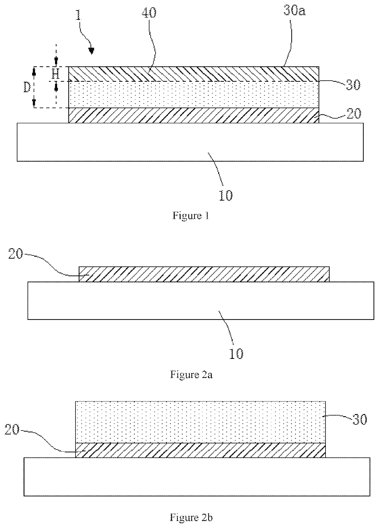
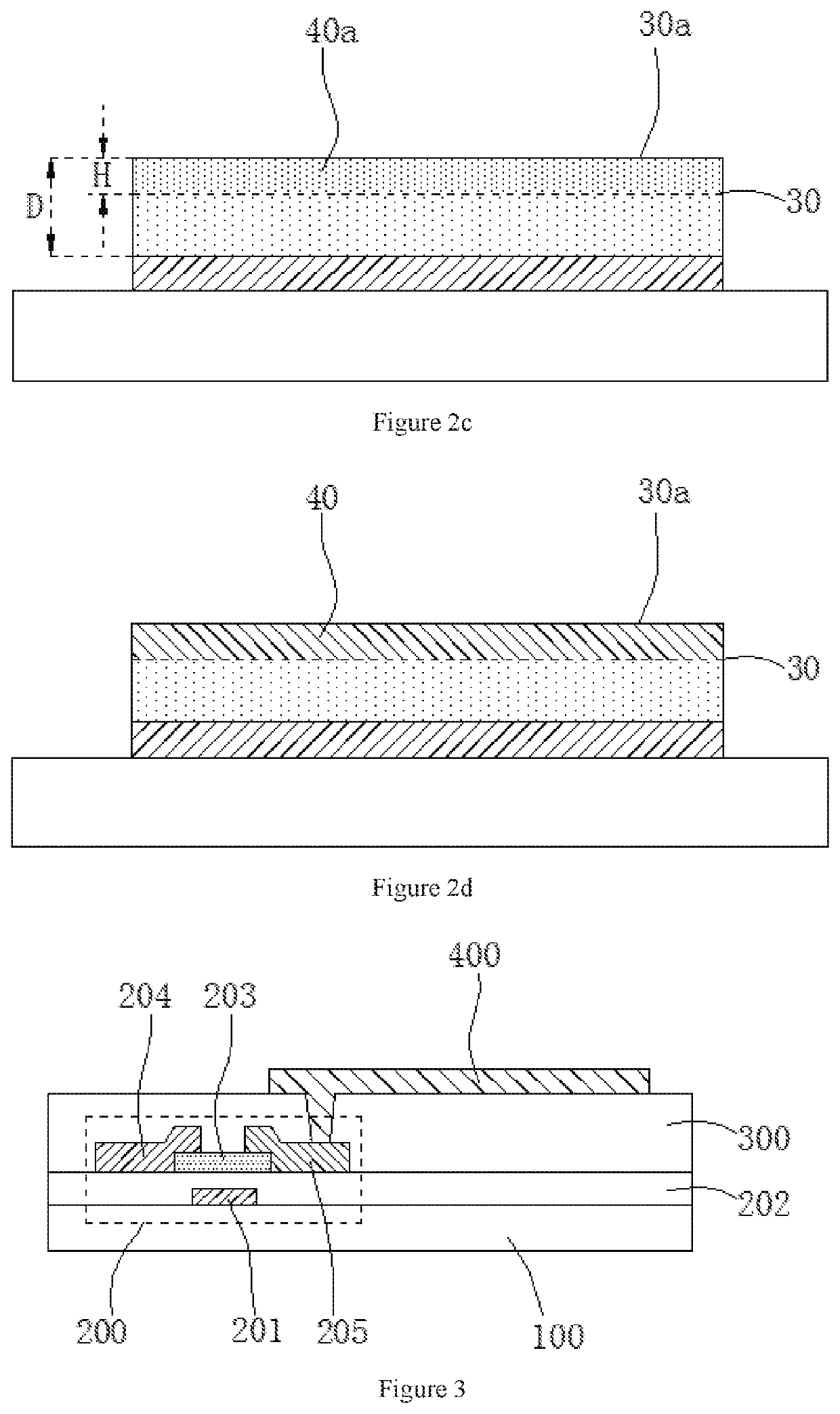
[0028]The present embodiment provides an electrode structure. As shown in FIG. 1, the electrode structure 1 comprises a copper metal layer 30 formed on a substrate 10, and the copper is used as a conductive functional layer of the electrode structure. The copper metal layer 30 is doped with a first metal ion within a range of a first depth H from an upper surface 30a. The first metal ion and the copper grain are combined by a metal bond to form a copper alloy layer 40. The upper surface 30a of the copper metal layer 30 refers to a surface of the copper metal layer 30 facing away from the substrate 10, and the first depth H is smaller than the thickness D of the copper metal layer 30. Specifically, the first metal ion is a metal ion having corrosion resistance and an ionic radius smaller than a gap between copper grains, and the first metal ion may be selected from one or more of the group of nickel (Ni) ions, tungsten (W) ions, and tantalum (Ta) ions.
[0029]In the present embodiment,...
embodiment 2
[0044]The present embodiment provides an array substrate. As shown in FIG. 3, the array substrate comprises a substrate 100, a TFT 200 and a pixel electrode 400 disposed on the substrate 100; a plurality of TFTs 200 is arranged in an array (only one of which is exemplarily shown in FIG. 3). The TFT array is disposed on the base substrate 100, and the TFT 200 is covered with a planarization layer 300, and the pixel electrode 400 is formed on the planarization layer 300. Each of the TFTs 200 is electrically connected to a pixel electrode 400 through a via provided in the planarization layer 300.
[0045]The TFT 200 comprises a gate electrode 201, a gate insulating layer 202, a semiconductor active layer 203, a source electrode 204, and a drain electrode 205. Specifically, as shown in FIG. 3, the gate electrode 201 is formed on the substrate 100, and the gate insulating layer 202 is formed on the substrate 100 and covers the gate electrode 201. The semiconductor active layer 203 is formed...
PUM
 Abstract
Description
Claims
Application Information