Liquid crystal display device
a liquid crystal display and display device technology, applied in non-linear optics, instruments, optics, etc., can solve the problem that the horizontal alignment mode liquid crystal display device cannot switch between on and off, and achieve the effect of suppressing light leakage, and reducing external light reflection
- Summary
- Abstract
- Description
- Claims
- Application Information
AI Technical Summary
Benefits of technology
Problems solved by technology
Method used
Image

Examples
embodiment 1
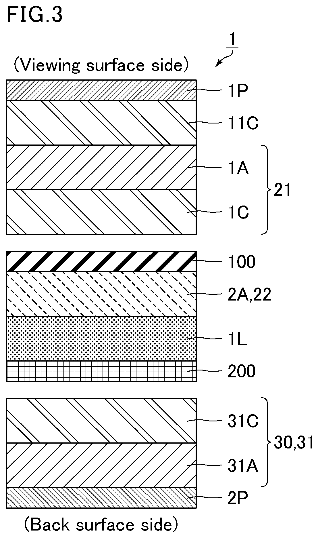
[0093]FIG. 2 is a schematic cross-sectional view of a liquid crystal display device of Embodiment 1. A liquid crystal display device 1 of the present embodiment includes, in the following order from the viewing surface side, a first polarizer 1P, a first positive A plate 1A having an in-plane retardation of 120 nm or greater and 155 nm or smaller, a positive C plate 1C having a thickness retardation of 80 nm or greater and 100 nm or smaller, a first substrate 100, a second positive A plate 2A having an in-plane retardation of 120 nm or greater and 155 nm or smaller, a horizontally aligned liquid crystal layer 1L, a second substrate 200, a viewing angle compensation layer 30, and a second polarizer 2P. The liquid crystal display device 1 further includes between the first polarizer 1P and the first positive A plate 1A a positive C plate 11C having a thickness retardation of 30 nm or greater and 80 nm or smaller.
[0094]The first substrate 100 includes, in the following order from the v...
embodiment 1-1
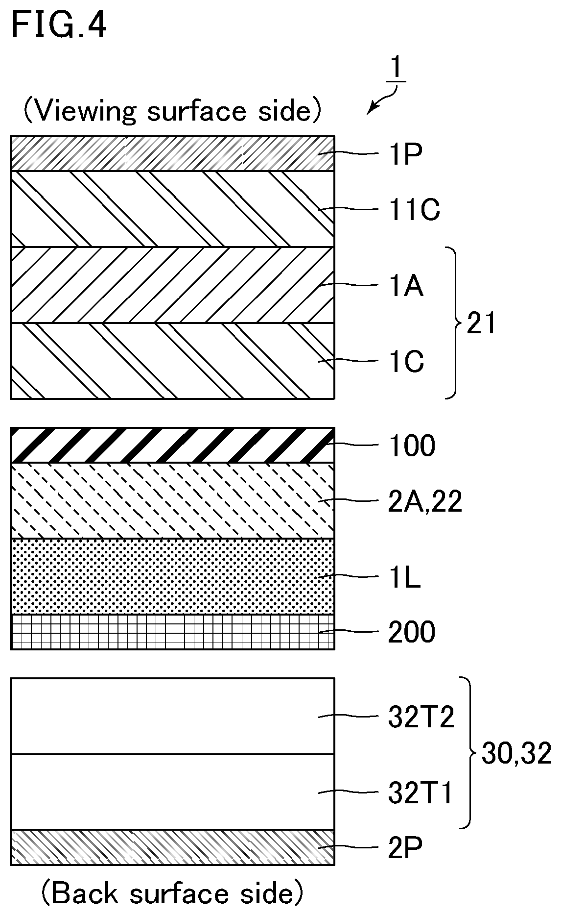
[0125]FIG. 3 is a schematic cross-sectional view of a liquid crystal display device of Embodiment 1-1. As shown in FIG. 3, the viewing angle compensation layer 30 in a liquid crystal display device 1 of the present embodiment is a first laminate 31 including, in the following order from the second polarizer 2P side, a positive A plate 31A having an in-plane retardation of 130 nm or greater and 150 nm or smaller and a positive C plate 31C having a thickness retardation of 80 nm or greater and 100 nm or smaller.
[0126]The positive A plate 31A has an in-plane retardation of preferably 132 nm or greater and 148 nm or smaller, more preferably 135 nm or greater and 145 nm or smaller.
[0127]The positive A plate 31A has an NZ coefficient of preferably 0.8 or greater and 1.2 or smaller, more preferably 0.9 or greater and 1.1 or smaller.
[0128]The positive A plate 31A may be formed by the same method as for the positive A plate 1A.
[0129]The positive C plate 31C has a thickness retardation of pre...
embodiment 1-2
[0132]FIG. 4 is a schematic cross-sectional view of a liquid crystal display device of Embodiment 1-2. As shown in FIG. 4, the viewing angle compensation layer 30 in a liquid crystal display device 1 of the present embodiment is a second laminate 32 including, in the following order from the second polarizer 2P side, a biaxial retardation layer 32T1 having an in-plane retardation of 80 nm or greater and 100 nm or smaller and an NZ coefficient of 1.3 or greater and 1.5 or smaller and a biaxial retardation layer 32T2 having an in-plane retardation of 50 nm or greater and 70 nm or smaller and an NZ coefficient of −1.2 or greater and −0.8 or smaller.
[0133]The biaxial retardation layer 32T1 may be formed by simultaneous biaxial stretching or sequential biaxial stretching on a material with a positive birefringence, for example. Specific examples of the material with a positive birefringence include the same as the examples for the materials of the resin film for a positive A plate.
[0134]...
PUM
| Property | Measurement | Unit |
|---|---|---|
| wavelength | aaaaa | aaaaa |
| polar angle θ | aaaaa | aaaaa |
| polar angle θ | aaaaa | aaaaa |
Abstract
Description
Claims
Application Information
 - R&D
- Intellectual Property
- Life Sciences
- Materials
- Tech Scout
- Unparalleled Data Quality
- Higher Quality Content
- 60% Fewer Hallucinations
Browse by: Latest US Patents, China's latest patents, Technical Efficacy Thesaurus, Application Domain, Technology Topic, Popular Technical Reports.
© 2025 PatSnap. All rights reserved.Legal|Privacy policy|Modern Slavery Act Transparency Statement|Sitemap|About US| Contact US: help@patsnap.com