Method for manufacturing a MEMS sensor

a manufacturing method and sensor technology, applied in the field of mems sensor, can solve the problem of reducing the area of the remaining mold surface, and achieve the effects of simple and reliable protection of the mems sensor, simple and cost-effective electrical contact, and simple detachment of the support layer

Active Publication Date: 2021-10-07
ROBERT BOSCH GMBH
View PDF0 Cites 0 Cited by
  • Summary
  • Abstract
  • Description
  • Claims
  • Application Information

AI Technical Summary

Benefits of technology

[0022]According to one further advantageous refinement of the present invention, an overmolding of the substrate and at least the MEMS structure takes place, in particular with the aid of transfer or compression molding. This allows for a simple and reliable protection of the MEMS sensor.
[0023]According to one further advantageous refinement of the present invention, contactings for the MEMS structure and / or for the ASIC element are situated on the front side of the substrate and the MEMS structure and / or the ASIC element are / is electrically contacted with the aid of wire bonding. This allows for a simple and cost-effective electrical contacting of the MEMS structure and / or the ASIC element.
[0024]According to one further advantageous refinement of the present invention, the support layer is removed after the overmolding. Therefore, the MEMS sensor may be easily placed into trays or as bulk material into containers, for example, for further processing.
[0025]According to one further advantageous refinement of the present invention, the support layer is acted upon by light in the UV range and / or thermally in order to be removed. The advantage thereof is that a simpler detachment of the support layer from the substrate is made possible.
[0026]According to one further advantageous refinement of the present invention, a plurality of cavities is formed, at least one MEMS structure being introduced into each of the cavities and, after the overmolding, a plurality of MEMS sensors being manufactured via separation according to the particular cavities, in particular with the aid of mechanical sawing in the direction from the front side toward the back side of the substrate. Therefore, a plurality of MEMS sensors may be manufactured in a simple and cost-effective way.
[0027]According to one further advantageous refinement of the present invention, at least one via is manufactured in the ASIC element, and the ASIC element and the MEMS structure are situated with respect to one another in such a way that the MEMS structure is electrically contacted with the aid of the at least one via of the ASIC element. This allows for a reliable contacting and a compact arrangement of the MEMS structure and the ASIC element.

Problems solved by technology

Due to the film-assisted molding, the chip usually protrudes from the molding compound and reduces the area of the remaining mold surface.

Method used


Image

  • Method for manufacturing a MEMS sensor
  • Method for manufacturing a MEMS sensor
  • Method for manufacturing a MEMS sensor

Examples


Embodiment Construction

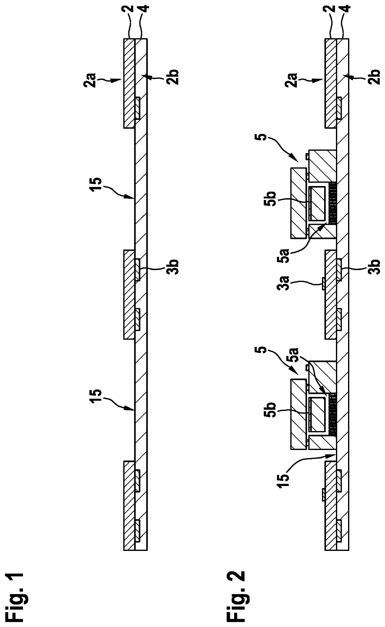
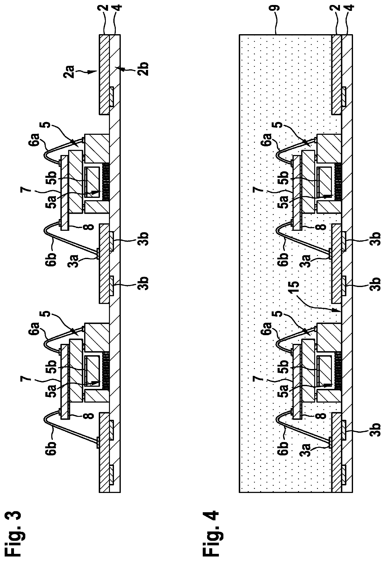
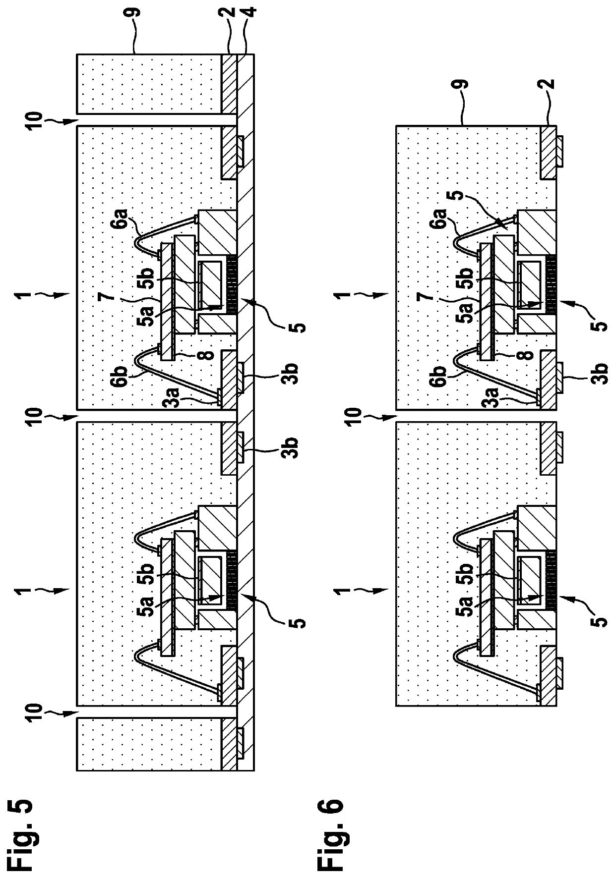
[0036]FIGS. 1 through 7 show steps of a method according to one specific example embodiment of the present invention.

[0037]FIGS. 1 through 7 show, in detail, steps of an example method for manufacturing a MEMS sensor 1. In FIG. 1, a substrate 2 is shown, which includes a temporarily situated carrier tape 4 on its back side 2b. Carrier tape 4, for example, in the form of a UV release tape, is laminated onto back side 2b of substrate 2. Carrier tape 4 includes, on the side facing substrate 2, an adhesive layer, which enables the adhesion between carrier tape 4 and substrate 2. Carrier tape 4 closes cavities 15 in substrate 2 from its back side 2b, as shown in FIG. 1. Substrate 2 also includes, on back side 2b, contactings 3b for the electrical contacting of substrate 2. These are completely enclosed by carrier tape 4.

[0038]In FIG. 2, MEMS structures 5 including accesses 5a for a functional layer 5b of particular MEMS structures 5 are now introduced into particular cavity 15. These may...


PUM

PropertyMeasurementUnit
gap heightaaaaaaaaaa
self-adhesiveaaaaaaaaaa
pressureaaaaaaaaaa

Abstract

A method for manufacturing a MEMS sensor. The method includes: providing a substrate, applying a support layer onto a back side of the substrate, forming at least one cavity in the substrate in such a way that an access to the back side from the front side is formed, introducing a MEMS structure into the at least one cavity, and fixing the MEMS structure on the support layer.

Description

FIELD[0001]The present invention relates to a method for manufacturing a MEMS sensor.[0002]Moreover, the present invention relates to a MEMS sensor.[0003]Although the present invention is applicable, in general, to arbitrary MEMS sensors, the present invention is described with respect to MEMS pressure sensors.BACKGROUND INFORMATION[0004]Conventional pressure sensors include a pressure-sensitive layer, for example, a diaphragm, which must remain in contact with the surroundings, in order to ensure a pressure access thereto. This pressure access is provided, in a conventional way, with the aid of so-called film-assisted molding and by, for example, a grid made up of small access holes on the top side of the chip of the pressure sensor. Due to the film-assisted molding, the chip usually protrudes from the molding compound and reduces the area of the remaining mold surface.[0005]German Patent Application No. DE 10 2016 220 077 A1 describes a method for manufacturing a micromechanical p...

Claims


Application Information

Patent Timeline
Patent Type & Authority Applications(United States)
IPC IPC(8): B81C1/00B81C3/00G01L19/00
CPCB81C1/00301B81C3/001B81C2203/037B81B2201/0264G01L19/0069B81C2203/0154B81B2207/012B81B2201/10B81C1/00309G01L19/06
Inventor SCHULER-WATKINS, SEBASTIANHAUG, DANIELHENN, TOBIAS
Owner ROBERT BOSCH GMBH
Why Eureka
Try Eureka