Packaging method and packaging structure of panel, and display device comprising packaging structure thereof

Inactive Publication Date: 2021-10-21
SHENZHEN CHINA STAR OPTOELECTRONICS SEMICON DISPLAY TECH CO LTD
View PDF0 Cites 0 Cited by
  • Summary
  • Abstract
  • Description
  • Claims
  • Application Information

AI Technical Summary

Benefits of technology

The invention provides a way to make a panel for display devices by covering a water-oxygen absorber and a redundant pixel region. This method effectively reduces the width of the panel's frame, resulting in a higher screen ratio and a narrower frame.

Problems solved by technology

This will make a frame of the panel too wide to achieve a narrow frame of the panel.

Method used


Image

  • Packaging method and packaging structure of panel, and display device comprising packaging structure thereof
  • Packaging method and packaging structure of panel, and display device comprising packaging structure thereof
  • Packaging method and packaging structure of panel, and display device comprising packaging structure thereof

Examples


first embodiment

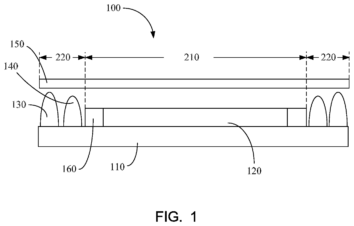
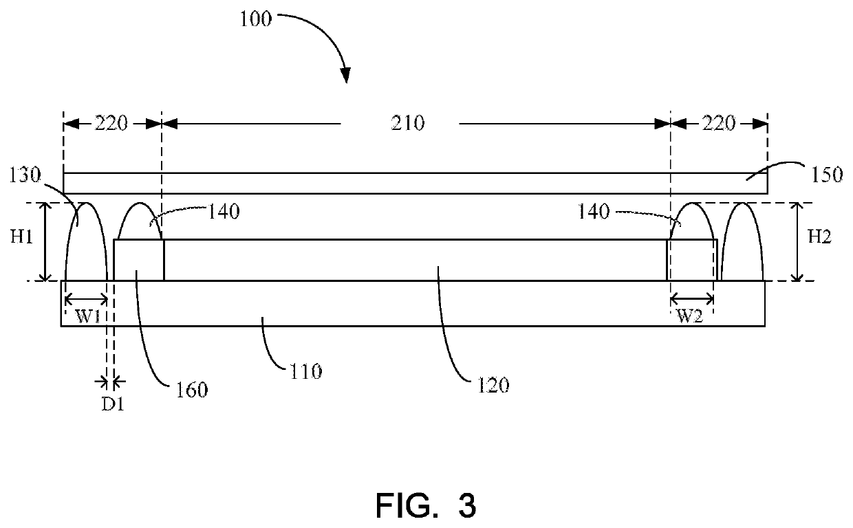
[0032]Preferably, in the first embodiment, a width W1 of the sealant 130 is between 0.1 mm and 3 mm, and a height H1 of the sealant 130 is between 3 um and 60 um. A width W2 of the water-oxygen absorber 140 is between 1 mm and 5 mm, and a height H2 of the water-oxygen absorber 140 is between 3 μm and 60 μm.

[0033]Therefore, when the water-oxygen absorber 140 is disposed on the redundant pixel region 160 of the OLED light-emitting device 120 in a fully covered manner, a size of the display region 210 can be effectively increased relative to the prior art, and a size of the non-display region 220 is reduced.

second embodiment

[0034]On the other hand, as shown in a second embodiment according to FIG. 4, the water-oxygen absorber 140 is disposed on the redundant pixel region 160 of the OLED light emitting device 120 in a partially covered manner. At this time, the distance D1 between the sealant 130 and the edge of the redundant pixel region 160 of the OLED light emitting device 120 is between 0.1 mm and 10 mm, and the distance D2 between the water-oxygen absorber 140 and the sealant 130 is between 0 mm and 3 mm.

[0035]Preferably, in the second embodiment, the width W1 of the sealant 130 is between 0.1 mm and 3 mm, and the height H1 of the sealant 130 is between 3 um and 60 um. The width W2 of the water-oxygen absorber 140 is between 1 mm and 5 mm, and the height H2 of the water-oxygen absorber 140 is between 3 μm and 60 μm.

[0036]Therefore, when the water-oxygen absorber 140 is disposed on the redundant pixel region 160 of the OLED light-emitting device 120 in a partially covered manner, the size of the dis...


PUM


Abstract

The present invention provides a packing method of a panel. The packing method of the panel includes following steps of: providing a substrate having an OLED light emitting device; coating a sealant around the OLED light emitting device; applying a water-oxygen absorber between the sealant and the OLED light emitting device; and aligning the substrate to cover a packaging glass cover for curing. Wherein, the water-oxygen absorber covers or partially covers a redundant pixel region of the OLED light emitting device to effectively reduce a width of a frame of the panel.

Description

FIELD OF INVENTION[0001]The present invention relates to the field of display technologies, and in particular, to a packaging method and a packaging structure of a panel, and a display device comprising the packaging structure.BACKGROUND OF INVENTION[0002]Organic light emitting diode (OLED) panels are an important direction for research and development of display devices, and have achieved remarkable results in applications such as small sizes and large sizes.[0003]However, in structures of OLED panels manufactured by inkjet printing technologies, redundant pixel regions with certain widths are generally required, so that an OLED light emitting device 120 can be uniformly formed within a film. Therefore, a frame of an inkjet printing panel generally at least comprises a circuit trace, a redundant pixel region, a packaging region, and the like.[0004]Therefore, as shown in FIG. 1, a panel comprises a display region 210 and a non-display region 220 disposed around the display region 21...

Claims


Application Information

Patent Timeline
IPC IPC(8): H01L51/52
CPCH01L51/5259H01L51/5246H10K59/10H10K50/846H10K50/8426
Inventor LI, XIANGLONGSINSUKE, IGUCHI
Owner SHENZHEN CHINA STAR OPTOELECTRONICS SEMICON DISPLAY TECH CO LTD
Why Eureka
Try Eureka