Array substrate and liquid crystal display

Active Publication Date: 2017-08-24
TRIVALE TECH
View PDF4 Cites 6 Cited by
  • Summary
  • Abstract
  • Description
  • Claims
  • Application Information

AI Technical Summary

Benefits of technology

The present invention provides an array substrate with a non-linear element to improve the performance of a display device. The non-linear element includes a light-shielding body, a first insulation film, a first oxide semiconductor film, a first source electrode, a first drain electrode, and a first back electrode. The first back electrode is connected to the source wire through a contact hole. The non-linear element provides high diode resistance and contributes to the reduced frame width of the display device.

Problems solved by technology

Thus, the liquid crystal display fails to drive liquid crystal molecules located above the pixel electrode sufficiently and has a low transmittance accordingly.
Thus, a short circuit arising from electrical breakdown or the like is more likely to occur between the source wire and the gate wire due to static electricity created in the manufacturing process.
The diode element increases in size due to such an increase in channel length, and a frame region of the array substrate expands accordingly, making it difficult to obtain an array substrate with a narrow frame.
While being processed, the oxide semiconductor layer included in the structure disclosed in Japanese Patent Application Laid-Open No. 2015-092601 is susceptible to etching damage, with a defect in the surface of the sidewall of the oxide semiconductor layer.
A leakage current is likely to occur in the defect.
In this structure, the channel length is short, so that the leakage current is more likely to occur, making it difficult to control resistance.

Method used


Image

  • Array substrate and liquid crystal display
  • Array substrate and liquid crystal display
  • Array substrate and liquid crystal display

Examples


first preferred embodiment

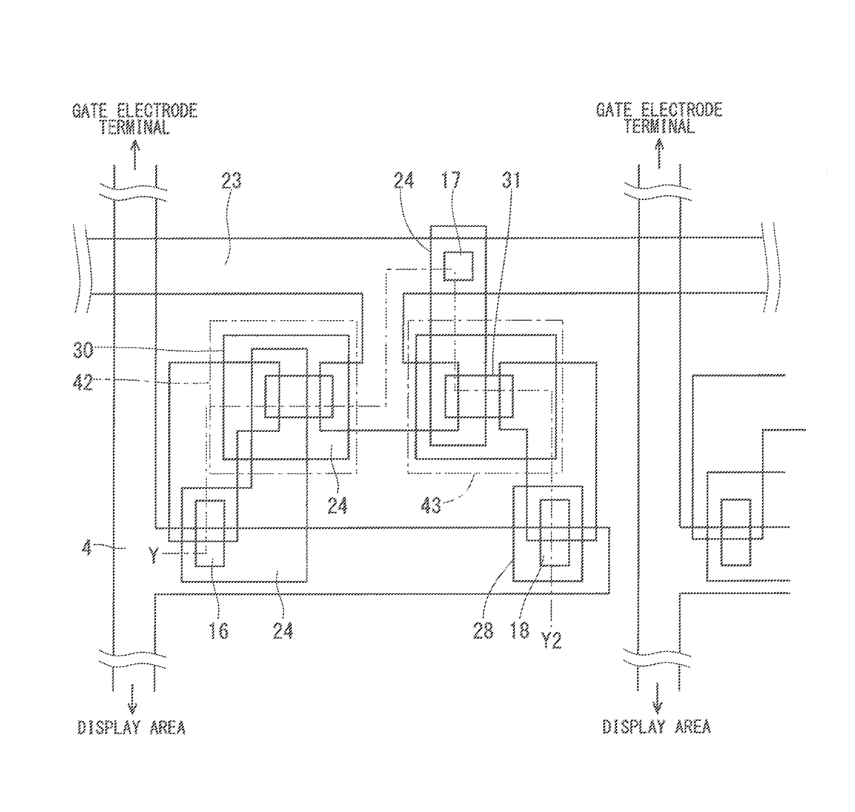
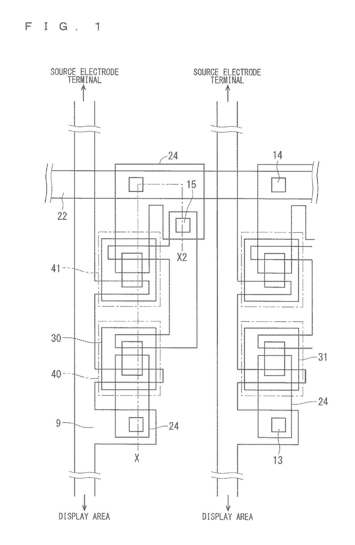
[0042]The following will describe a configuration of a non-linear element (bidirectional diode) connected to a source wire.

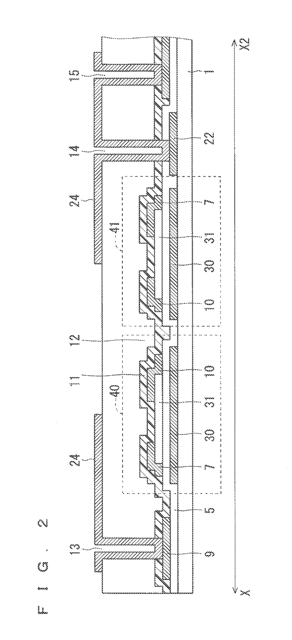
[0043]FIG. 1 is a plan view of an example configuration of a bidirectional diode adjacent to a source wire according to a first preferred embodiment of the present invention. FIG. 2 is a cross-sectional view taken along the line X-X2 of FIG. 1.

[0044]As illustrated in FIGS. 1 and 2, a light-shielding body 30 and a short ring wire 22, which are formed by processing a first conducive film made of metal or the like, are located on a substrate 1. The substrate 1 is a transparent insulation substrate made of, for example, glass. Here, the first conductive film is used to form a low-resistance wire that is to be formed into the short ring wire 22. Alternatively, the low-resistance wire may be formed of a second conductive film, which will be described below.

[0045]The light-shielding body 30 and the short ring wire 22 are covered with a first insulation film 5 (a first ...

second preferred embodiment

[0065]The following will describe another configuration of the non-linear element (the bidirectional diode) connected to the source wire.

[0066]FIG. 5 is a plan view of an example configuration of the bidirectional diode adjacent to the source wire according to a second preferred embodiment of the present invention. FIG. 6 is a cross-sectional view taken along the line A-A2 of FIG. 5.

[0067]As illustrated in FIGS. 5 and 6, the light-shielding body 30 and the short ring wire 22, which are formed by processing the first conductive film made of metal or the like, are located on the substrate 1 that is a transparent insulation substrate made of, for example, glass. Here, the first conductive film is used to form a low-resistance wire that is to be formed into the short ring wire 22. Alternatively, the low-resistance wire may be formed of the second conductive film, which will be described below.

[0068]The first insulation film 5 is formed so as to cover the light-shielding body 30 and the ...

third preferred embodiment

[0084]The following will describe a third preferred embodiment of the present invention, in which the non-linear element (the bidirectional diode) in the second preferred embodiment is applied to an array substrate for the FFS mode (hereinafter referred to as an “FFS” array substrate). The bidirectional diode according to the second preferred embodiment is highly compatible with the FFS array substrate. The second electrode 25, the third back electrode 26, and a liquid crystal driving electrode (the pixel electrode or the common electrode) on the FFS array substrate can be formed as one layer and can be formed of the same material. The liquid crystal driving electrode is located on an organic insulation film, and thus, the FFS array substrate can achieve high aperture ratio. On such an FFS array substrate, a protection circuit including the back electrodes can be formed, with no additional process.

[0085]FIG. 9 is a plan view of an example configuration of an FFS array substrate acco...


PUM


Abstract

An array substrate according to the present invention includes a non-linear element. The non-linear element includes a first insulation film disposed so as to cover a light-shielding body, an oxide semiconductor film disposed on the first insulation film so as to overlap the light-shielding body in a plan view, a source electrode and a drain electrode that are disposed so as to be apart from each other with a separation portion therebetween on the oxide semiconductor film, a second insulation film disposed so as to cover the oxide semiconductor film, the source electrode, and the drain electrode, and a first back electrode disposed on a third insulation film and connected to a source wire through a first contact hole. The first back electrode is disposed so as to overlap the source electrode and part of the separation portion on the oxide semiconductor film in a plan view.

Description

BACKGROUND OF THE INVENTION[0001]Field of the Invention[0002]The present invention relates to an array substrate including a non-linear element and also relates to a liquid crystal display including the array substrate.[0003]Description of the Background Art[0004]Common examples of liquid crystal display modes include the twisted nematic (TN) mode and the transverse electric field mode for achieving a wide viewing angle and a high contrast, such as the in-plane switching mode and the fringe field switching (FFS) mode. Liquid crystal displays employing the IPS mode perform display by applying a transverse electric field to liquid crystals sandwiched between opposed substrates. In such a liquid crystal display, a pixel electrode and a common electrode to which the transverse electric field is applied are located on the same layer. Thus, the liquid crystal display fails to drive liquid crystal molecules located above the pixel electrode sufficiently and has a low transmittance accordin...

Claims


Application Information

Patent Timeline
IPC IPC(8): G02F1/1368G02F1/1333G02F1/1343H01L27/12G02F1/1362
CPCG02F1/1368H01L27/124H01L27/1225G02F1/136209G02F1/134309G02F2201/121G02F1/136227G02F2202/10G02F2001/134372G02F2202/02G02F2201/124G02F1/133345H01L27/1222H01L27/1259H01L29/417H01L29/861G02F1/136204G02F1/134372H01L27/1244H01L29/78633H01L29/7869
Inventor ODA, KOJI
Owner TRIVALE TECH
Why Eureka
Try Eureka