Array substrate

a substrate and array technology, applied in the field of array substrates, can solve the problems of inability to maintain a high level for a long time, goa cannot output ultra-wide pulses, cascaded transmission circuits will also fail, etc., to achieve the effect of reducing the outputting pulse width of the goa circuit, reducing the pulse width, and high level

Active Publication Date: 2021-11-18
SHENZHEN CHINA STAR OPTOELECTRONICS SEMICON DISPLAY TECH CO LTD
View PDF0 Cites 1 Cited by
  • Summary
  • Abstract
  • Description
  • Claims
  • Application Information

AI Technical Summary

Benefits of technology

[0018]The beneficial effect of the present invention is that the array substrate of the present invention includes a GOA circuit and a plurality of logic AND gate units integrated in a rear end of the GOA circuit, wherein the GOA circuit includes a plurality of cascaded GOA units, each of the GOA units includes a scan terminal, and at least three cascaded GOA units are connected to one of the logic AND gate units through the scan terminals. When the circuit is in operation, at least three cascaded GOA units can be successively raised to a high level, so that the output signal terminal of the logic AND gate unit can maintain a high level for a longer time. The array substrate of the invention can reduce the outputting pulse width of the GOA circuit, and the reduction of the pulse width can reduce the leakage current of the first node (Q), and is favorable for obtaining a stable GOA outputting signal, and the GOA circuit can be normally cascaded at the same time.
[0019]In order to illustrate the technical solutions of the present disclosure or the related art in a clearer manner, the drawings desired for the present disclosure or the related art will be described hereinafter briefly. Obviously, the following drawings merely relate to some embodiments of the present disclosure, and based on these drawings, a person skilled in the art may obtain the other drawings without any creative effort.
[0020]FIG. 1 is a signal waveform diagram of a current array substrate.
[0021]FIG. 2 is a schematic structural diagram showing an array substrate according to an embodiment of the present invention.
[0022]FIG. 3 is a schematic circuit diagram of an array substrate according to an embodiment of the present invention.
[0023]FIG. 4 is a signal waveform diagram of an array substrate according to an embodiment of the present invention.

Problems solved by technology

If a leakage current of thin film transistor (TFT) is large, the node Q cannot maintain a high level for a long time, and the GOA cannot output the ultra-wide pulse.
Therefore, the GOA circuit cannot output a wide pulse, and at the moment, the actual pulse width of the GOA circuit is 2 ms; and since the pulse width of the GOA circuit is less than 3 ms, a cascaded transmission of the circuit will also fail.

Method used


Image

  • Array substrate
  • Array substrate
  • Array substrate

Examples


Embodiment Construction

[0027]The following description of each embodiment, with reference to the accompanying drawings, is used to exemplify specific embodiments which may be carried out in the present invention. Directional terms mentioned in the present invention, such as “top”, “bottom”, “front”, “back”, “left”, “right”, “inside”, “outside”, “side”, etc., are only used with reference to the orientation of the accompanying drawings. Therefore, the used directional terms are intended to illustrate, but not to limit, the present invention. In the drawings, components having similar structures are denoted by the same numerals.

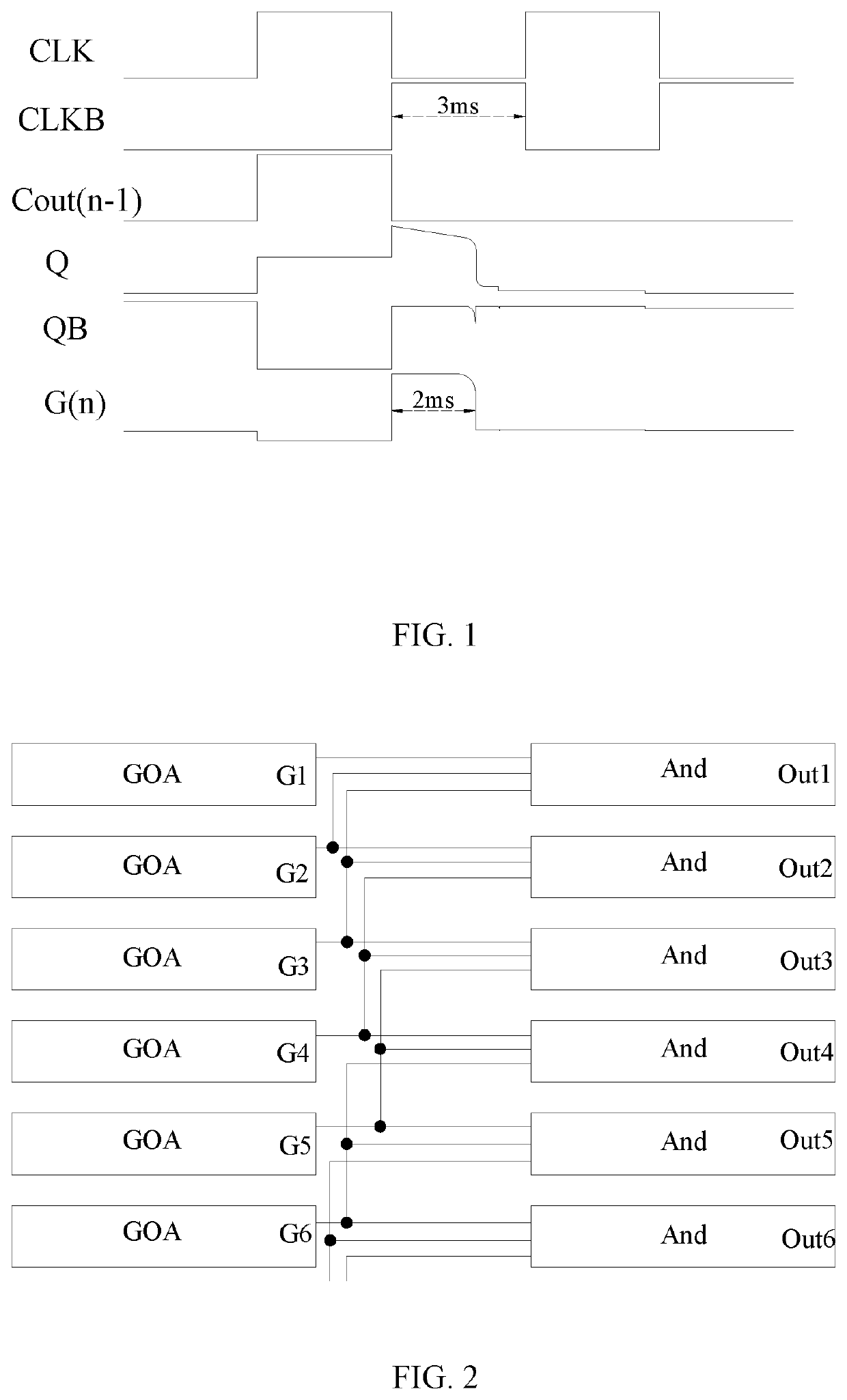
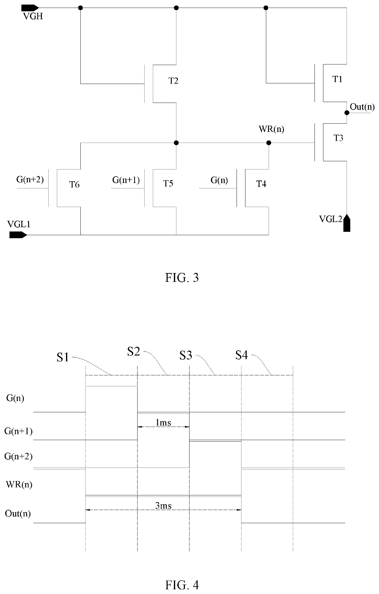
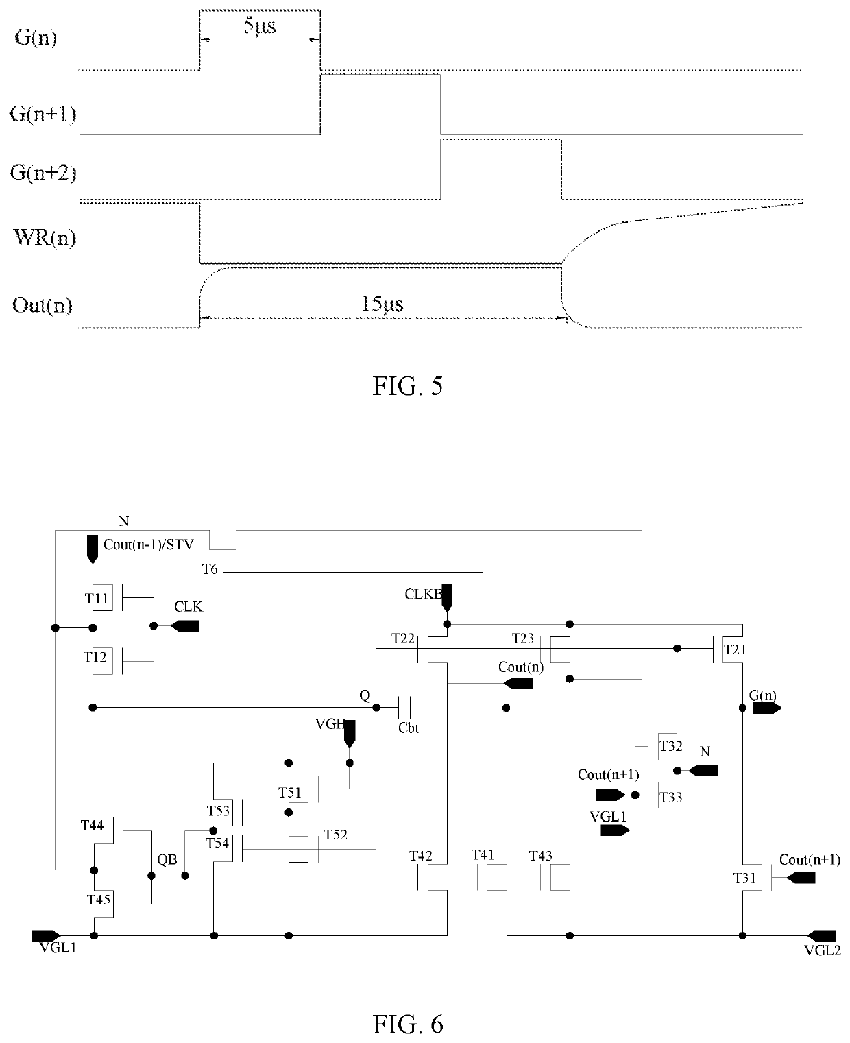
[0028]The present embodiment can solve the technical problem that a node Q of array substrate currently cannot maintain high level for a long time due to a large leakage current of thin film transistor (TFT), and a gate driver on array (GOA) cannot output the ultra-wide pulse.

[0029]As shown in FIG. 2, the present invention provides an array substrate, the array substrate includes a GO...


PUM


Abstract

An array substrate is provided, which includes a gate driver on array (GOA) circuit and a plurality of logic AND gate units integrated in a rear end of the GOA circuit. The GOA circuit includes a plurality of cascaded GOA units, each of the GOA units includes a scan terminal, and continuous at least three cascaded GOA units are connected to one of the logic AND gate units through the scan terminals.

Description

FIELD OF INVENTION[0001]The present invention relates to a field of display technologies, and in particular, to an array substrate.BACKGROUND OF INVENTION[0002]Organic light-emitting diodes (OLED) display device can be classified into two types: passive matrix OLED (PMOLED) and active matrix OLED (AMOLED) according to the driving method. Among them, an AMOLED has pixels arranged in an array, belongs to an active display type, has high luminous efficiency, and is generally used as a high-definition large-sized display device.[0003]At present, large-size AMOELD panel generally adopt an external compensation scheme for the pixels, and the external compensation scheme requires a gate driver on array (GOA) circuit to output an ultra-wide pulse signal (>3 millisecond (ms)). Therefore, in an output stage, a first node (Q) of the GOA circuit needs to maintain a wide pulse width for a long time, and at this time, the node Q is in a floating state. If a leakage current of thin film transis...

Claims


Application Information

Patent Timeline
Patent Type & Authority Applications(United States)
IPC IPC(8): G09G3/3266
CPCG09G3/3266G09G2300/0814G09G2300/0408G11C19/28G09G2230/00G09G2320/0214
Inventor XUE, YAN
Owner SHENZHEN CHINA STAR OPTOELECTRONICS SEMICON DISPLAY TECH CO LTD
Why Eureka
Try Eureka