

Transient Voltage Protection for Low Voltage Circuits
a technology of transient voltage protection and low voltage, applied in the direction of aircraft static dischargers, pv power plants, emergency protective arrangements for limiting excess voltage/current, etc., can solve the problems of low voltage node being susceptible to failur
- Summary
- Abstract
- Description
- Claims
- Application Information
AI Technical Summary
Benefits of technology
Problems solved by technology
Method used
Image

Examples
Embodiment Construction
[0015]The Figures and the following description describe certain embodiments by way of illustration only. One of ordinary skill in the art will readily recognize from the following description that alternative embodiments of the structures and methods illustrated herein may be employed without departing from the principles described herein. Reference will now be made in detail to several embodiments, examples of which are illustrated in the accompanying figures.
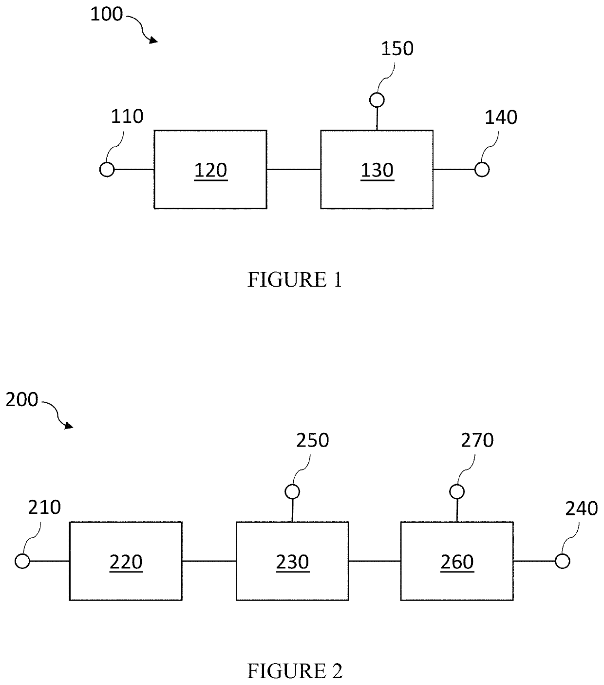
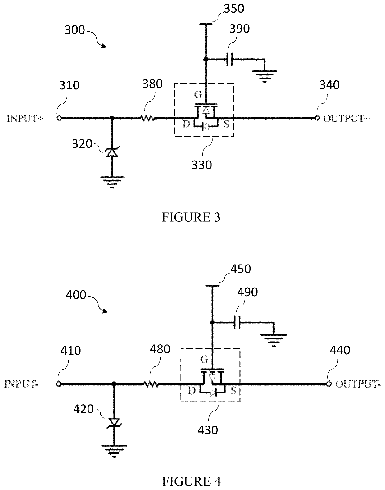
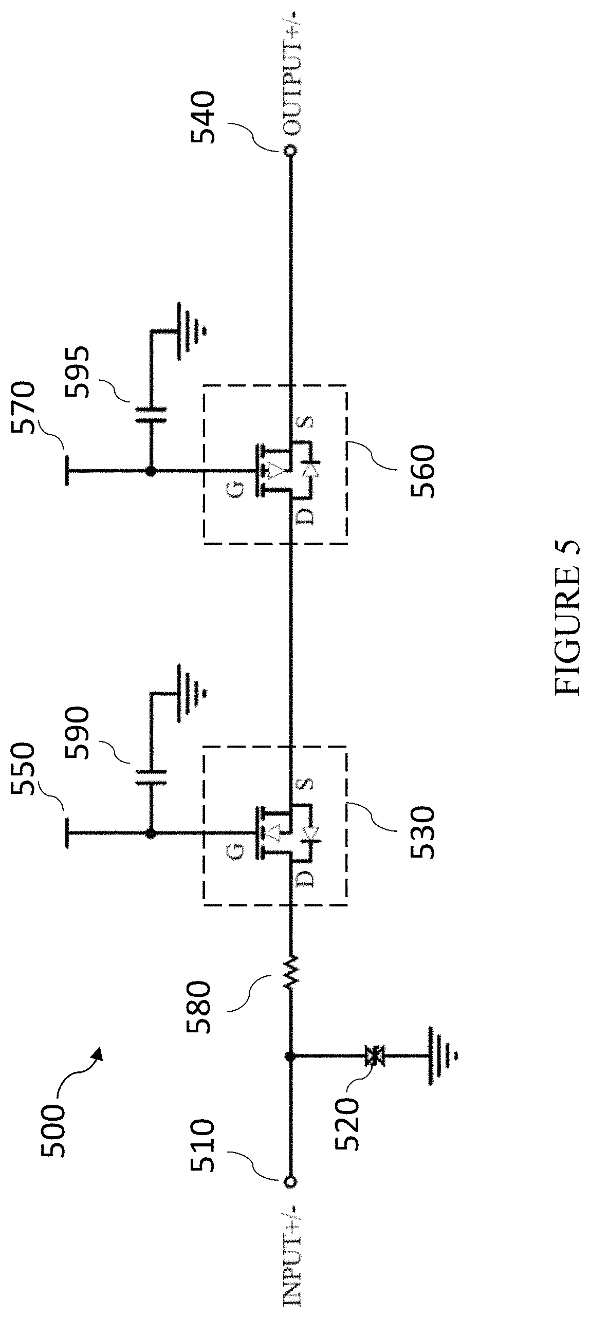
[0016]The present invention is directed to transient voltage protection for low voltage circuits using a transient voltage suppression (TVS) element (e.g., a TVS diode) in serial with a transistor, such as an N-channel metal-oxide-semiconductor field-effect transistor (MOSFET), a P-channel MOSFET, or another type of field-effect transistor (FET). In some cases, both an N-channel and a P-channel MOSFET can be used in serial with a bidirectional TVS diode. Many low voltage level circuits or nodes have a small range of operating...
PUM
| Property | Measurement | Unit |
|---|---|---|
| voltage | aaaaa | aaaaa |
| operating voltages | aaaaa | aaaaa |
| operating voltages | aaaaa | aaaaa |
Abstract
Description
Claims
Application Information