Pixel circuit and pixel control method
a pixel circuit and control method technology, applied in the direction of instruments, static indicating devices, etc., can solve the problems of complicated circuit configuration, variable luminance, complicated pixel circuit, etc., and achieve the effect of quick control of pixels and simple configuration
- Summary
- Abstract
- Description
- Claims
- Application Information
AI Technical Summary
Benefits of technology
Problems solved by technology
Method used
Image

Examples
first embodiment
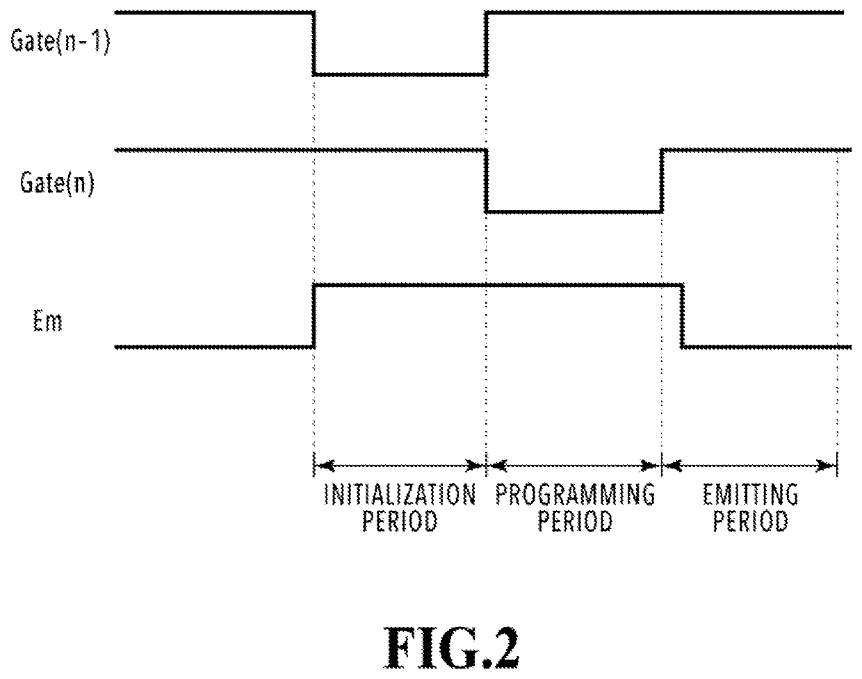
[0071]First, the operational principle of the present embodiment will be described with reference to FIGS. 1 to 4.
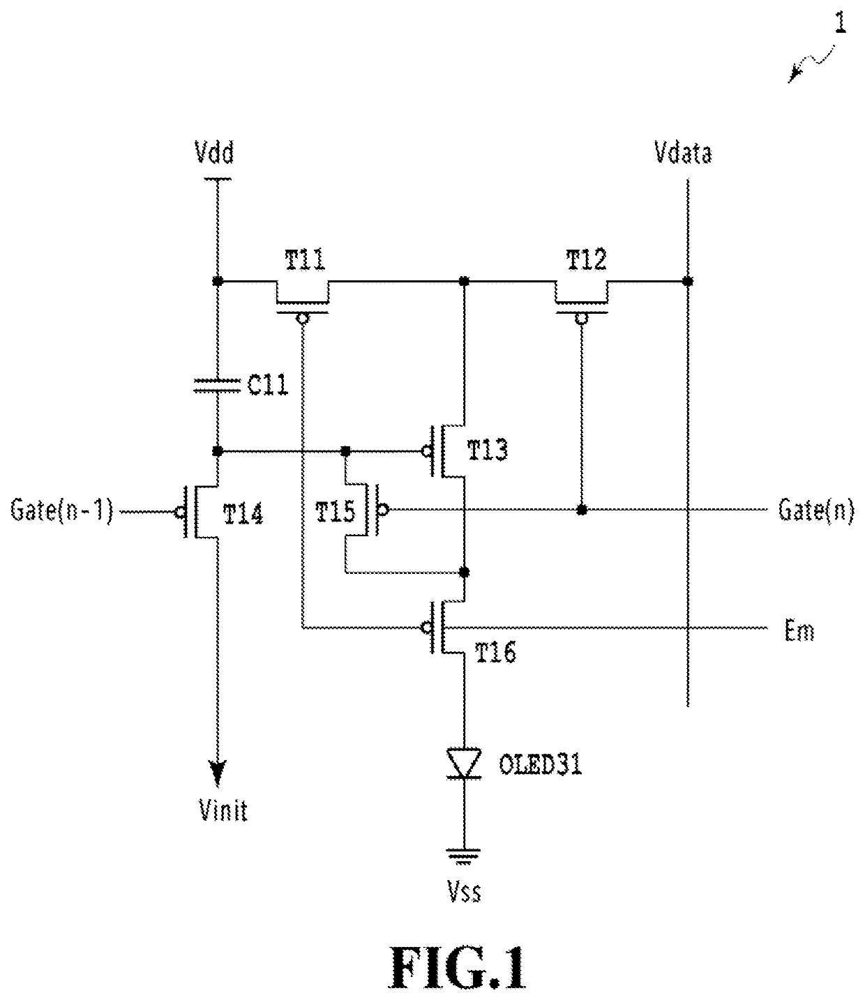
[0072]FIG. 1 is a diagram showing an example of the configuration of a 6T1C circuit which is a pixel unit drive circuit used in an OLED. This pixel unit drive circuit 1 drives and controls pixels for each pixel unit, and one subpixel corresponds to a pixel unit in the following description. This pixel unit drive circuit 1 includes one OLED 31, six transistors T11 to T16, and one capacitor C11. One OLED 31 corresponds to a subpixel of one color of red (R), green (G) and blue (B) subpixels constituting one pixel.
[0073]The pixel unit drive circuit 1 includes the switching transistor T12 for, in response to a scan (gate) signal Gate(n) applied to the nth scan line, switching a data signal of a voltage level Vdata applied to the corresponding data line. The pixel unit drive circuit 1 also includes the driving transistor T13 that supplies a drive current for the OLED 31 accord...
second embodiment
[0107]FIG. 11 is a diagram showing the configuration of a pixel circuit 11 including a combination of a pixel unit drive circuit 501 and an image sensor 110 according to another embodiment of the present invention. The pixel circuit 11 differs from the pixel circuit 5 shown in FIG. 5 in that the pixel circuit 11 does not have the reset transistor T58. In this embodiment, the PD 58 is reset by controlling the bias voltage VPD on the cathode side of the PD 58.
[0108]Procedures of a pixel control method that is executed by the pixel circuit 11 shown in FIG. 11 will be described with reference to a timing chart in FIG. 12. Operations in the initialization period and the PD read period are the same as the operations described above with reference to FIG. 6. In the PD reset period, as indicated by a circle 1201, the bias voltage VPD goes low at the same time as the anode potential AND goes low. When the anode potential AND is set high and the bias voltage VPD is set low by controlling the ...
third embodiment
[0111]FIGS. 13 to 15 are timing charts for describing an example of controlling the frequency of resetting the PD 58 in the above-described pixel circuit. In FIGS. 13 to 15, Gaten−1 and Gaten−2 respectively indicate the first scan signal and the second scan signal on the nth scan line. Further, numerals added to Em1, VPD1, AND1, etc. indicate the number of scan line.
[0112]FIG. 13 shows an example where in an OLED having a refresh rate of 60 Hz, data writing to the OLED and resetting and reading of the PD are performed at the same frequency sequentially for each of four scan lines. Normally, data writing to the OLED takes about 1 μs. As mentioned above, when resetting and reading of the PD are added between resetting and writing of the OLED every time, the data writing interval becomes longer accordingly. In the case of a display with 2000 to 3000 scan lines, slow display operation becomes prominent.
[0113]Accordingly, in the present embodiment, the frequency of resetting and reading ...
PUM
 Abstract
Description
Claims
Application Information
 - R&D
- Intellectual Property
- Life Sciences
- Materials
- Tech Scout
- Unparalleled Data Quality
- Higher Quality Content
- 60% Fewer Hallucinations
Browse by: Latest US Patents, China's latest patents, Technical Efficacy Thesaurus, Application Domain, Technology Topic, Popular Technical Reports.
© 2025 PatSnap. All rights reserved.Legal|Privacy policy|Modern Slavery Act Transparency Statement|Sitemap|About US| Contact US: help@patsnap.com