
Method of manufacturing semiconductor structure and semiconductor structure

a manufacturing method and technology of semiconductors, applied in the direction of semiconductor devices, electrical appliances, basic electric elements, etc., can solve the problem of the active area continuing to shrink

Inactive Publication Date: 2022-02-03
NAN YA TECH
View PDF4 Cites 1 Cited by
  • Summary
  • Abstract
  • Description
  • Claims
  • Application Information

AI Technical Summary

Benefits of technology

The present patent discusses a method to make a semiconductor structure that can address the issue of active regions becoming misaligned.

Problems solved by technology

As semiconductor devices become smaller and highly integrated, the pitch of the active areas continue to shrink.
However, shrinkage of the pitch of the active areas and shrinkage of the size of the isolation structure may cause some problems, such as toppling of the active areas during processes of forming the isolation structure.

Method used


Image

  • Method of manufacturing semiconductor structure and semiconductor structure
  • Method of manufacturing semiconductor structure and semiconductor structure
  • Method of manufacturing semiconductor structure and semiconductor structure

Examples


Embodiment Construction

[0030]In order that the present disclosure is described in detail and completeness, implementation aspects and specific embodiments of the present disclosure with illustrative description are presented, but it is not the only form for implementation or use of the specific embodiments of the present disclosure. The embodiments disclosed herein may be combined or substituted with each other in an advantageous manner, and other embodiments may be added to an embodiment without further description. In the following description, numerous specific details will be described in detail in order to enable the reader to fully understand the following embodiments. However, the embodiments of the present disclosure may be practiced without these specific details.

[0031]Further, spatially relative terms, such as “beneath,”“over,” and the like, may be used herein for ease of description to describe one element or feature's relationship to another element(s) or feature(s) as shown in the figures. Th...


PUM

PropertyMeasurementUnit
widthaaaaaaaaaa
width w1aaaaaaaaaa
width w1aaaaaaaaaa

Abstract

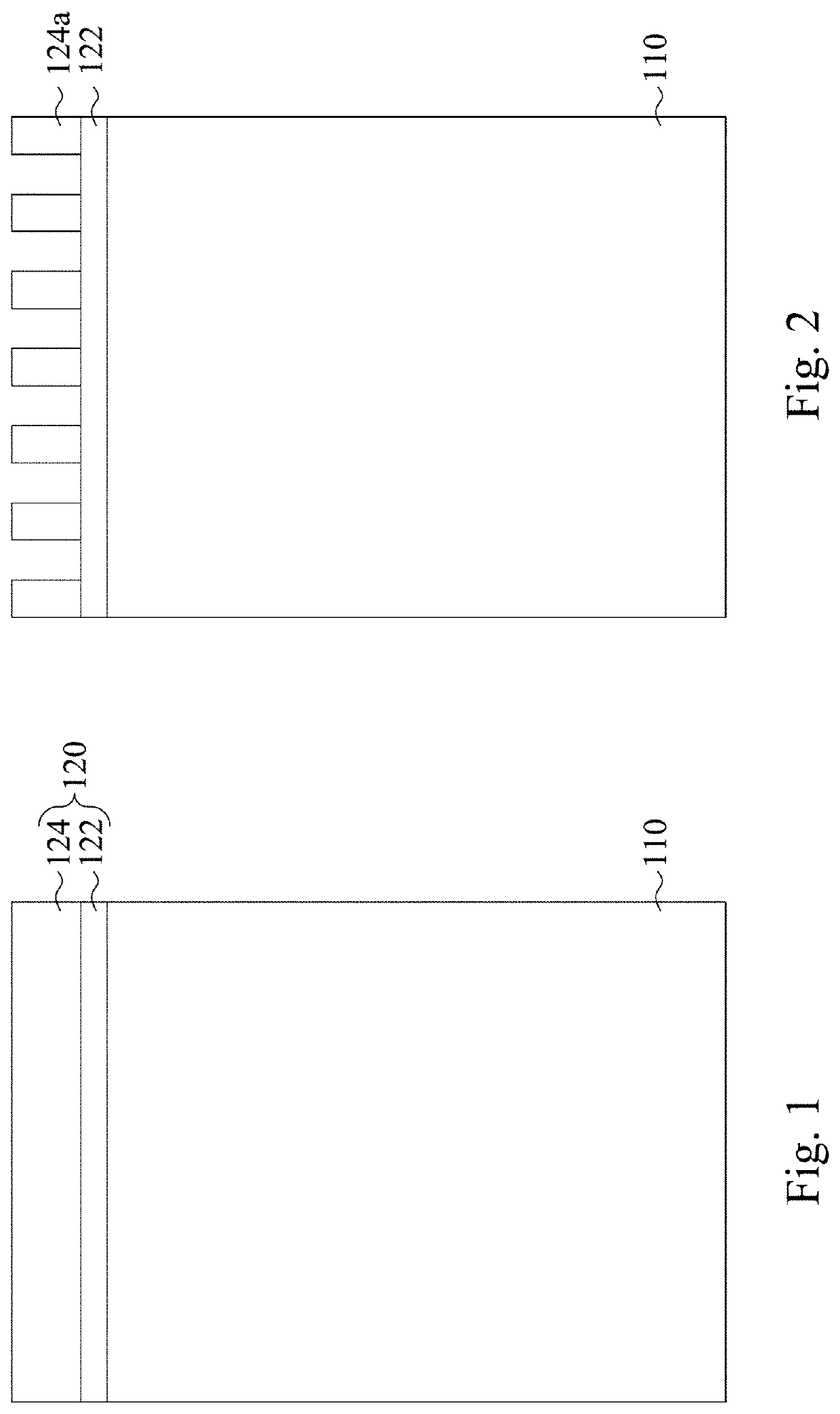
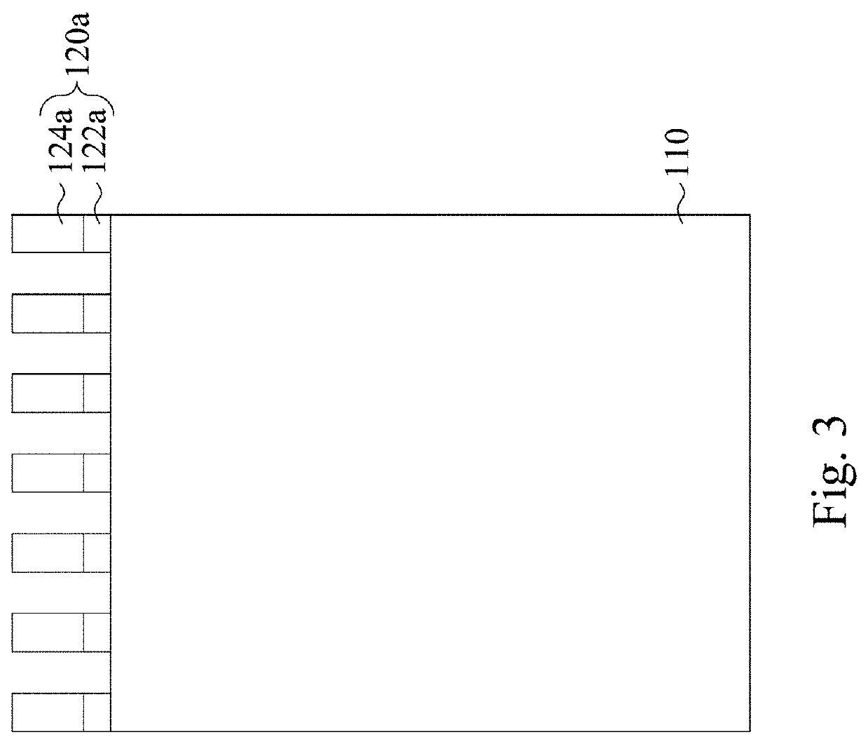
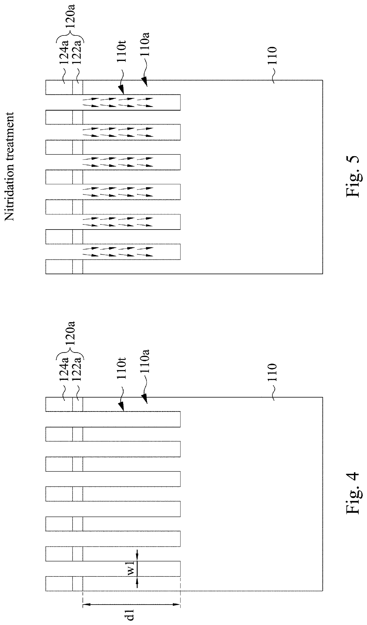
A method of manufacturing a semiconductor structure includes: etching a substrate according to a hard mask to form a plurality of trenches in the substrate; performing a nitridation treatment on the trenches of the substrate; filling the trenches of the substrate with a flowable isolation material; and solidifying the flowable isolation material to form an isolation material. A semiconductor structure manufactured by the method is also provided.

Description

BACKGROUNDField of Invention[0001]The present invention relates to a method of manufacturing a semiconductor structure and a semiconductor structure.Description of Related Art[0002]In a semiconductor device, an isolation structure is formed between active areas (AA) for electrically insulated the active areas. As semiconductor devices become smaller and highly integrated, the pitch of the active areas continue to shrink. Accordingly, the size of the isolation structure continues to shrink as well.[0003]However, shrinkage of the pitch of the active areas and shrinkage of the size of the isolation structure may cause some problems, such as toppling of the active areas during processes of forming the isolation structure.SUMMARY[0004]The present invention provides a method of manufacturing a semiconductor structure which can solve the issue of toppling of active regions.[0005]In accordance with an aspect of the present invention, a method of manufacturing a semiconductor structure inclu...

Claims


Application Information

Patent Timeline
Patent Type & Authority Applications(United States)
IPC IPC(8): H01L21/762
CPCH01L21/76237H01L21/02247H01L21/76227H01L29/0649H01L21/02222H01L21/02282H01L21/0217H01L21/02271H01L21/76224H01L21/02252H01L21/02255H01L21/02304H01L21/02238
Inventor CHUANG, YING-CHENGLIAO, CHE-HSIEN
Owner NAN YA TECH
Learn More